Piezoresistive Pressure Sensor Temperature Drift Compensation Mechanics
Dual-mode compensation pairing constant current excitation with digital polynomial modeling suppresses piezoresistive thermal drift to 0.1 percent full scale.


Carrier
Silicon crystal diaphragms deform under applied pressure, redistributing charge transport pathways across diffused semiconductor resistors. In a p-type piezoresistive element aligned along the crystalline direction of a (100) silicon wafer, longitudinal tensile stress alters the valence band degenerate energy states. Heavy-hole and light-hole sub-bands split under mechanical strain.
This band deformation shifts hole populations between bands of differing effective mass, producing an immediate change in electrical resistivity. The magnitude of this piezoresistive response depends on fundamental solid-state parameters that shift dramatically across operating temperatures.
P-type resistors show positive resistance coefficients. As lattice temperature rises from negative 40 degrees Celsius to 125 degrees Celsius, thermal vibrations agitate the crystal grid. Acoustic phonon scattering intensifies, reducing hole mobility throughout the diffused resistor volume.
Because electrical resistivity equals the reciprocal of the product of charge, carrier density, and carrier mobility, this reduction in mobility increases the base electrical resistance of the piezoresistor. The Temperature Coefficient of Resistance (TCR) defines this positive slope, typically running between positive 0.12 percent per degree Celsius and positive 0.28 percent per degree Celsius for typical boron doping profiles. Pure silicon exhibits high piezoresistive response.
Uncompensated sensors experience substantial baseline impedance elevation when exposed to hot media.
Under constant 5.0-volt bridge excitation, a 100-kilopascal piezoresistive die with a boron doping level of 5e18 atoms per cubic centimeter exhibits a 21.4 percent span reduction across the temperature excursion from 20 degrees Celsius to 125 degrees Celsius.
Thermal sensitivity degradation exhibits an opposite trajectory. The fundamental piezoresistive coefficient, designated pi-44 in cubic silicon symmetry, governs the conversion of mechanical stress into fractional resistance change. Thermal expansion of the energy bandgap and thermal carrier distribution across splitting sub-bands diminish the piezoresistive coupling efficiency as temperature climbs.
The fractional piezoresistive coefficient decreases monotonically with rising temperature, establishing a negative Temperature Coefficient of Sensitivity (TCS). Depending on dopant density, uncompensated bridge span drops between negative 0.14 percent per degree Celsius and negative 0.24 percent per degree Celsius. Piezoresistive pressure transmitters driven by fixed voltage sources lose signal amplitude in elevated temperature environments.

Doping Concentration Trade-Offs in Silicon
Boron implantation into p-type sensing elements governs both baseline electrical resistivity and thermal sensitivity. Heavy doping attenuates temperature drift at the expense of raw gauge factor. When boron concentration exceeds 1e19 atoms per cubic centimeter, impurity scattering begins to dominate acoustic phonon scattering, flattening the carrier mobility curve across temperature.
Gauge factors drop precipitously under heavy boron loading, reducing open-circuit bridge sensitivity. Sensor designers balance thermal coefficient magnitude against baseline signal output during die fabrication.
| Boron Density (atoms/cm³) | Resistivity (ohm-cm) | Piezoresistive Pi-44 (1e-11 Pa⁻¹) | TCR (%/°C) | TCS (%/°C) |
|---|---|---|---|---|
| 1.0e18 | 0.082 | 102.5 | +0.09 | -0.27 |
| 5.0e18 | 0.021 | 84.0 | +0.16 | -0.21 |
| 1.0e19 | 0.011 | 67.5 | +0.22 | -0.16 |
| 5.0e19 | 0.003 | 38.0 | +0.28 | -0.08 |
Boron concentration dictates mobility drop. Sensor dies fabricated with light doping yield strong full-scale bridge outputs reaching 100 to 150 millivolts at room temperature, yet their negative TCS requires aggressive gain compensation over industrial spans. Dies doped beyond 5e19 atoms per cubic centimeter limit span drift below 8 percent across an 80-degree thermal window, but generate full-scale outputs below 40 millivolts.
Slower signal-to-noise ratios follow this lower output, challenging the resolution limits of subsequent analog-to-digital converters.
Whether sub-band splitting under triaxial packaging stress creates non-linear carrier scattering models that invalidate standard piezoresistive mobility matrices at cryogenic limits remains an open research question across deep-well MEMS geometries.


Joint
Mechanical assembly introduces the dominant portion of thermal zero shift in micromachined pressure dies. Silicon exhibits a low linear coefficient of thermal expansion (CTE) of approximately 2.6 parts per million per degree Celsius at room temperature. The structural members supporting the silicon chip, including glass pedestals, ceramic headers, metallic housings, and adhesive bonding layers, exhibit disparate expansion behaviors.
Thermal excursions generate significant bimetallic bending stresses across the interface, projecting parasitic mechanical strain directly into the flexible silicon diaphragm. The Wheatstone bridge converts these mounting stresses into output voltage indistinguishable from applied fluid pressure.
Thermal mismatch warps the silicon plate. Die attach adhesives creep under thermal cycling. When a sensor die mounts directly to an alumina carrier with a CTE of 6.5 parts per million per degree Celsius using rigid epoxy, the adhesive layer contracts aggressively during cool-down from its curing temperature.
The resulting shear stress propagates through the bulk silicon into the diaphragm perimeter. Piezoresistors positioned adjacent to the diaphragm edges experience localized compressive or tensile prestress. Because resistor geometries and doping distributions vary across microfabrication tolerances, stress fields affect individual bridge arms unevenly, generating substantial thermal zero offset drift (TCO).
A symmetry breakdown of 0.05 percent in nominal resistance across four bridge arms produces an uncompensated zero shift exceeding two percent of full-scale span across an 80-degree Celsius gradient.
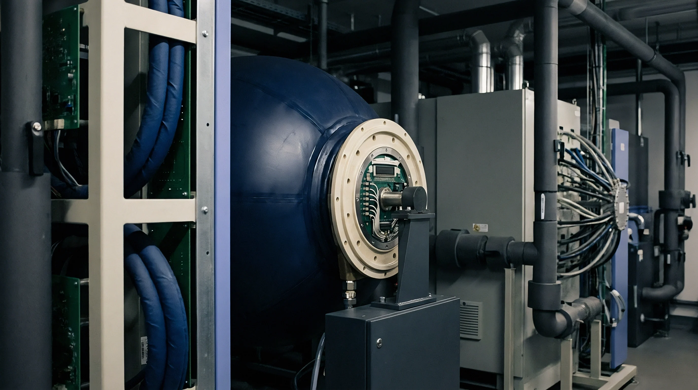
Thermal Expansion Mismatch in Sensor Packaging
Differential shrinkage between borosilicate glass pedestals, silicon substrates, and metallic headers creates bending moments across the sensing membrane. Borosilicate glass such as Schott 8330 or Corning 7740 matches silicon expansion over a narrow window near 25 degrees Celsius, yet departs substantially above 100 degrees Celsius and below zero. Anodic bonding fuses the glass constraint to the silicon wafer at 350 to 400 degrees Celsius under an applied electrostatic field.
Freezing this joint at high temperature locks residual tension into the assembly upon cooling to room temperature. When the operating environment shifts, this frozen stress state relaxes or amplifies, causing the diaphragm to cup upward or downward independent of process pressure.
- Asymmetric Adhesive Bleedout generates non-uniform boundary clamping along die edges, inducing twisting moments across the diaphragm that rotate piezoresistive axes out of optimal crystalline alignment.
- Substrate Voiding creates localized thermal insulation pockets beneath the die, allowing transient temperature gradients between opposing bridge arms during rapid fluid temperature shifts.
- Package Moisture Swelling alters the volume of transfer-molded epoxy encapsulants over time, translating hygroscopic swelling stresses through leadframes directly into sensitive membrane margins.
- Bond Wire Differential Pull exerts micro-gram mechanical vectors on metallization pads when thick aluminum or gold bond wires expand against rigid silicone gel potting compounds.
| Material Layer | CTE (ppm/°C) | Elastic Modulus (GPa) | Typical Thickness (µm) | Zero Drift Contribution (%FS) |
|---|---|---|---|---|
| Monocrystalline Silicon | 2.6 | 169 | 350 | Baseline |
| Borosilicate Glass (Pyrex 7740) | 3.2 | 64 | 1000 | 0.35 to 0.80 |
| Filled Epoxy Die Attach | 35.0 | 6.5 | 25 | 1.20 to 3.50 |
| Soft Silicone Elastomer | 300.0 | 0.002 | 50 | 0.05 to 0.15 |
| Alumina Ceramic (96% Al₂O₃) | 6.5 | 310 | 800 | 0.90 to 2.10 |
| Kovar Alloy Header | 5.8 | 138 | 1500 | 0.70 to 1.80 |
Soft silicone adhesives isolate mounting strains through low elastic modulus, dampening stress transfer from external housings into the die. Silicones introduce outgassing risks and permit die movement under intense vibration. High-modulus epoxies anchor the die firmly against mechanical shock, transmitting destructive thermal strains that warp thin diaphragms.
Gold wire bonds introduce thermal differentials. Selection of mounting layers dictates the repeatability of zero drift profiles over operating lifecycles.
Neglecting adhesive viscoelastic relaxation curves during enclosure design causes irreversible zero drift calibration errors that exceed the sensor operating accuracy budget within hundreds of thermal cycles in the field.


Shunt
Passive compensation networks balance bridge parameter shifts by manipulating excitation bias or inserting temperature-dependent resistance paths. Analog methods avoid digital processor overhead, delivering continuous, noise-free compensation inside the front-end analog circuit domain. Bridge topology, excitation mode, and discrete component placement fix the stability envelope of these classic compensation mechanics.
Driving the piezoresistive bridge with a constant current source yields natural span compensation. The bridge input resistance exhibits a positive TCR, climbing steadily with increasing temperature. Under a constant current supply, the excitation voltage across the bridge terminals rises in direct proportion to this resistance growth: V equals I multiplied by R-bridge.
The negative TCS of the piezoresistors reduces bridge output per unit of excitation voltage as temperature rises. The simultaneous increase in total bridge voltage counteracts this sensitivity drop. Constant current supply stabilizes bridge sensitivity.
When TCR magnitude closely matches the absolute value of TCS, passive sensitivity stabilization occurs without supplemental correction components.
Constant current excitation attenuates span drift by a factor of five compared to raw constant voltage drive across industrial operating ranges.
Span compensation tracks total resistance change. The self-compensation mechanism falters when manufacturing variations cause TCR and TCS magnitudes to diverge. For diffused boron resistors, TCR values often measure around positive 0.16 percent per degree Celsius, whereas TCS values measure approximately negative 0.21 percent per degree Celsius.
The sensitivity loss outpaces the terminal voltage rise, leaving residual negative span drift across elevated temperatures. Passive networks resolve this imbalance by placing fixed precision resistors and thermistors into parallel and series configurations with the bridge elements.

Where Does Passive Trimming Fail across Wide Temperature Spans?
Laser cutting of thick-film metal traces resolves zero offset at a single room calibration point. A fixed resistor added in series with an individual bridge arm equalizes baseline imbalances, eliminating room-temperature offset voltages. Thermal zero drift, however, exhibits higher-order non-linear behavior driven by packaging stress curvature and temperature-dependent dopant activation.
A static series trim resistor possesses a negligible temperature coefficient compared to the diffused silicon resistors. As temperature swings away from the trim point, the mismatched temperature coefficients between the thin-film trim resistor and the active silicon arm introduce secondary zero drift gradients.
- Constant Current Supply with Series Span Resistor drops the effective excitation growth rate, compensating sensors where the base TCR exceeds the absolute TCS value.
- Parallel Shunt Resistor across Bridge Terminals diverts a fraction of the constant current bias as temperature rises, preventing bridge terminal overvoltage in high-impedance transducer dies.
- Thermistor-Resistor Quadrant Network inserts positive or negative temperature coefficient elements directly into the offset correction loop to bend first-order zero drift slopes back toward baseline.
- Operational Amplifier Active Feedback Loop samples bridge current through an external sensing element to actively adjust bridge drive voltage according to analog transfer functions.
Analog trims leave second-order curvature uncorrected. Precision sensors operating over broad spans from negative 40 degrees Celsius to 125 degrees Celsius exhibit parabolic span and offset profiles. Discrete resistor networks linearize endpoint errors, leaving substantial intermediate bowing across the mid-temperature range.
Calibrating these networks demands labor-intensive iterative trimming: technicians or automated lasers cut resistors, run the module through a thermal cycle, calculate error curves, and trim secondary correction rungs. Thermal settling times consume substantial bench resources.
Suppliers frequently defend residual mid-band drift by asserting that analog trimming networks meet catalog endpoint accuracy specifications, omitting the fact that thermal bowing across intermediate temperature bands exceeds the endpoint band by a factor of three.


Algorithm
Mixed-signal conditioning circuits digitize bridge millivolt outputs and internal diode voltages through high-resolution converters. Dedicated sensor interface ASICs bypass the physical compromises of passive analog networks by converting compensation into mathematical execution. High-resolution delta-sigma analog-to-digital converters, low-noise programmable gain instrumentation amplifiers, and on-chip digital signal processing cores extract raw differential bridge signals alongside die temperature measurements, correcting thermal zero and span errors in firmware.
The on-chip temperature sensor must track the piezoresistive membrane thermal state without spatial or temporal lag. Standard conditioning architectures embed a forward-biased p-n junction diode or a specialized diffused silicon resistance element directly into the sensor die periphery. Diode forward voltage decreases linearly with temperature at approximately negative 2.0 millivolts per degree Celsius when driven by a stable current bias.
An auxiliary ADC channel samples this diode voltage synchronously with primary bridge measurements. The digital processing core reads both raw digital values and applies corrective arithmetic matrices derived during factory calibration.
A standard second-order compensation matrix evaluates pressure as the sum of uncorrected pressure plus temperature-dependent zero offset and span correction terms across every conversion cycle.
Polynomial coefficients occupy on-chip memory registers. The correction engine computes compensated pressure output through Taylor series expansions modeling bridge behavior across pressure and temperature domains. The mathematical relationship models both thermal zero shift and thermal span degradation, including cross-coupling terms where sensitivity drift varies as a function of instantaneous pressure.

Which Polynomial Order Balances Calibration Time and Residual Error?
Mathematical modeling of semiconductor bridges balances manufacturing test overhead against acceptable field accuracy. Linear first-order compensation requires testing each device at only two temperatures, such as 25 degrees Celsius and 85 degrees Celsius. This model calculates a single offset slope and a single span gain factor, halving test bench occupancy.
Second-order polynomial models require a minimum of three distinct temperature test points to compute quadratic curvature coefficients, capturing parabolic die-attach thermal stress and non-linear mobility decay. Third-order fits eliminate residual ‘S’ curvature.
- Raw Bridge Signal Conversion digitizes differential millivolt outputs through a low-noise 24-bit delta-sigma converter with programmable gain scaling.
- Die Temperature Extraction reads on-chip diode forward voltage drops to determine local substrate junction temperature within 0.1 degrees Celsius precision.
- Zero Offset Evaluation calculates the baseline shift polynomial from stored calibration coefficients, subtracting thermal offset from raw pressure counts.
- Sensitivity Correction Scaling divides offset-corrected pressure values by the temperature-dependent span polynomial to normalize sensor gain across the full operational envelope.
- Output Protocol Serialization formats linearized pressure data into I2C, SPI, SENT, or 4-20 milliamp analog output frames for transmission to host control modules.
| Model Topology | Minimum Calibration Points (P × T) | Floating-Point Operations per Cycle | Residual Total Error Band (%FS) | Calibration Time per Batch (Hours) |
|---|---|---|---|---|
| First-Order Linear | 2 × 2 = 4 | 4 | ±1.50 to ±2.50 | 1.2 |
| Second-Order Polynomial | 3 × 3 = 9 | 11 | ±0.25 to ±0.50 | 3.5 |
| Third-Order Polynomial | 4 × 4 = 16 | 22 | ±0.05 to ±0.15 | 6.8 |
| 2D Look-Up Table (Interpolated) | 5 × 5 = 25 | 16 | ±0.02 to ±0.08 | 11.4 |
Two-dimensional Look-Up Tables (LUT) store discrete error matrices within non-volatile EEPROM memory. During run-time operations, the ASIC identifies the bounding pressure and temperature grid coordinates, executing bilinear interpolation between adjacent nodes. Look-up tables accommodate irregular, non-monotonic thermal stress profiles that defy third-order polynomial fits, such as localized packaging stress inversions induced by glass transition phases in potting adhesives.
Look-up tables demand dense multi-point factory calibration matrices that inflate testing time.
According to standard industrial sensor supply agreements incorporating DIN EN 60770-1 validation criteria, digital compensation accuracy ratings are nullified when thermal slew rates exceed supplier-specified limits, transferring complete liability for dynamic temperature gradient errors to the system integrator.
Execution rates in digital signal conditioning ASICs run between 500 Hertz and 10 kilohertz. High oversampling ratios inside the delta-sigma core filter high-frequency thermal noise, but introduce signal group delay into fast pressure transient monitoring. Engineers balance digital filter cutoff frequencies against allowable output ripple when configuring front-end registers for dynamic hydraulic or combustion applications.

Yield
Multi-point environmental chamber cycling represents the primary production bottleneck for calibrated silicon transducers. While wafer-scale microfabrication produces tens of thousands of raw sensor dies simultaneously at low unit cost, packaging and thermal calibration proceed sequentially or in small batch matrices. Loading assembled transducers into environmental test chambers, applying stabilized reference pressures, and dwelling until internal thermal equilibrium occurs consumes substantial electrical energy, machine time, and facility footprint.
Thermal calibration costs routinely exceed the combined cost of the silicon die, ceramic substrate, and protective metal housing.
Chamber stabilization dominates overall test time. Production ovens cycle through three distinct plateaus. Transducers mounted onto pressure manifolds inside thermal chambers cannot be measured during active temperature transitions.
Internal thermal gradients between the outer stainless steel shell, the internal silicone oil fill, and the embedded silicon die generate false thermal transient offsets. Calibrators hold the chamber at target temperatures until internal thermocouples confirm stability within 0.2 degrees Celsius over five consecutive minutes. A three-temperature calibration cycle at negative 40, positive 25, and positive 125 degrees Celsius demands two to four hours of chamber dwell time per batch.
Facility throughput dictates factory margins. Sensor manufacturers configure multiplexed pressure manifolds containing hundreds of sensor sockets to maximize batch size. Manifold volume increases pneumatically with every added port, increasing the gas volume required to cycle through pressure calibration points.
Leaks in manifold O-rings, pneumatic valving drift, or electrical contact resistances inside cryogenic sockets ruin entire calibration runs, forcing lots back through secondary test passes or landing them in scrap bins.
Incoming inspection protocols verify polynomial calibration stability by subjecting sample batches to thermal envelope audits. Transducers undergo baseline verification at ambient conditions, enter a thermal test chamber stepped across the operating range, and report pressure under calibrated deadweight testers. Unstable die attach bonds, micro-cracks in glass pedestals, or contaminated silicon surfaces reveal themselves through thermal hysteresis: the sensor reports differing pressure values at 25 degrees Celsius depending on whether it arrived from negative 40 degrees Celsius or positive 125 degrees Celsius.
Digital polynomial compensation engines cannot correct thermal hysteresis because the sensor output ceases to be a single-valued function of temperature.
Supply contracts referencing ISO 10012 measurement management standards enforce that calibration coefficients stored in sensor non-volatile memory must survive specified thermal shock cycles without exhibiting zero offset migrations exceeding 0.1 percent of span, obligating suppliers to replace entire manufacturing lots when batch sample units demonstrate post-stress coefficient wander.