Polymer Die Attach Stress Mitigation in Capacitive Accelerometers
Optimizing soft silicone or filler-modified die attach materials and dot dispensing configurations mitigates thermo-mechanical strain in capacitive MEMS dies.


Substrate
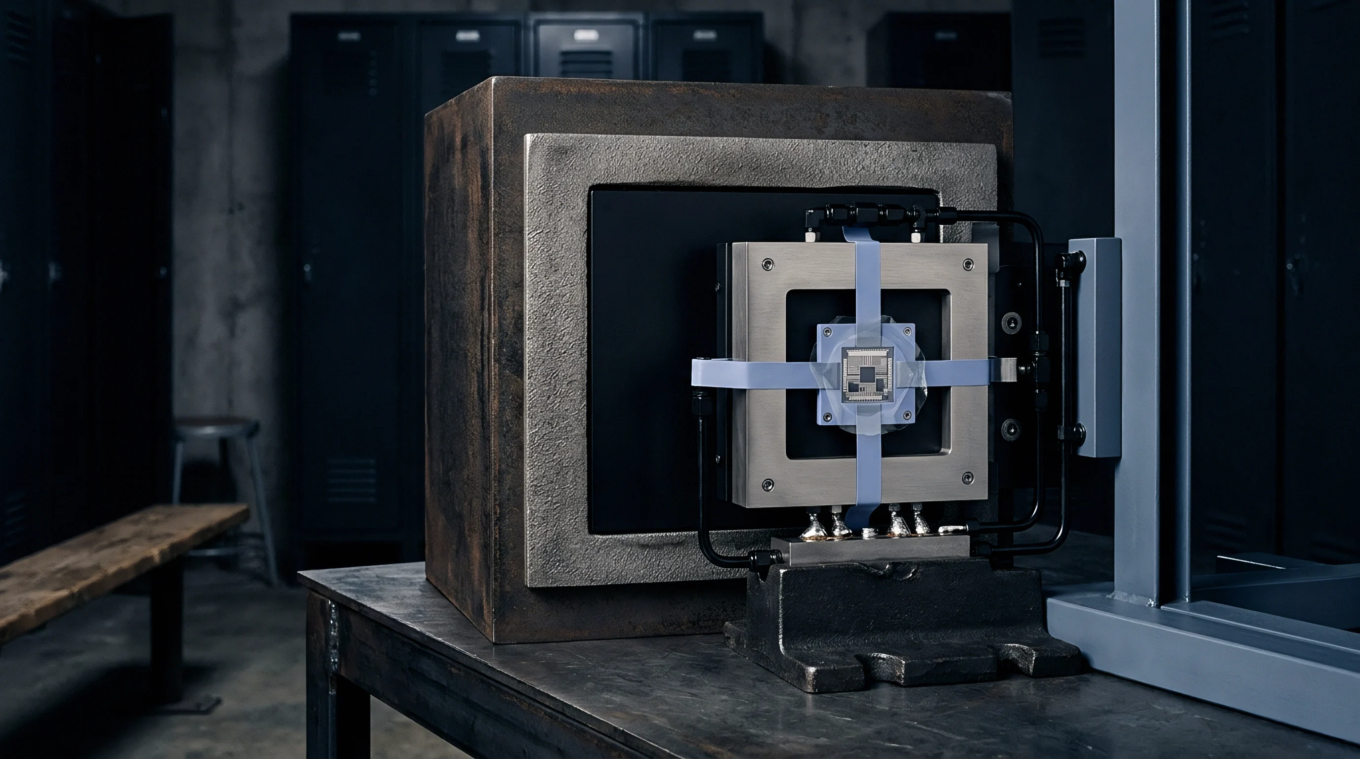
Mechanical coupling between a silicon sensing die and package materials converts ambient thermal expansion into differential mechanical strain. In capacitive micro-electromechanical sensors, micro-machined interdigitated comb structures detect acceleration through sub-nanometer shifts in differential gap distances. Silicon exhibits a coefficient of thermal expansion of 2.6 parts per million per degree Celsius at room temperature.
Copper leadframes expand at 16.5 parts per million per degree Celsius, while organic FR4 substrates expand at 14 to 17 parts per million per degree Celsius. Bonding a rigid silicon element directly to an organic carrier using high-modulus structural adhesives locks in thermo-mechanical strain during post-cure cooling.
When environmental temperatures drift during sensor operation, expansion differentials deform the underlying silicon substrate. Bending moments applied to the chip plane alter the resting distance between fixed stator fingers and movable rotor fingers. A gap change as small as 0.1 nanometer across a nominal 1.2-micrometer capacitive gap induces a measurable zero-g bias shift.
Thermal gradients across the package produce asymmetric strain gradients, shifting sensor outputs independently of applied kinetic acceleration.

Thermo-Mechanical Strain Coupling Mechanics
Differential expansion across package interfaces transfers shear forces into the silicon comb structures. The primary vector of stress transfer originates at the lower bond line, where the adhesive layer acts as the physical bridge between package leadframe and micro-machined silicon. High shear modulus polymers, such as conventional filled epoxies with moduli exceeding 3.0 gigapascals, transfer upwards of 85 percent of substrate strain into the active silicon layer.
Substrate mismatch drives baseline drift. The magnitude of die flexure scales directly with the distance from the neutral center of the die. Outer sensing combs experience higher mechanical displacement than central combs.
Linear expansion mismatch generates spherical or parabolic die curvature depending on package symmetry. In dual-axis or three-axis capacitive sensors, parabolic curvature creates cross-axis sensitivity by tilting the suspended proof mass anchor points relative to the ground plane.
A 40-micrometer silicone die attach bond line limits zero-g offset shift to under 0.15 milligrahs per degree Celsius between minus forty and plus one hundred twenty-five degrees Celsius.
Uncontrolled thermal gradients warp comb fingers. Lowering the transferred strain demands engineered compliance within the die attach layer or structural isolation within the silicon layout itself. Shear forces concentrate along outer chip margins.
Standard failure modes arising from unmitigated die attach strain in capacitive motion sensors exhibit consistent electromechanical symptoms:
- Zero-G Offset Thermal Drift Shifts in quiescent capacitive output voltage observed during uniform thermal ramps across specified operating ranges.
- Thermal Hysteresis Residual baseline offset variation recorded after returning to ambient temperature following thermal cycling.
- Axis Cross-Sensitivity Spikes Mechanically induced tilting of proof mass suspensions generating false signal outputs on orthogonal sensing channels.
- Capacitance Non-Linearity Strain-induced warping of comb geometries altering the baseline inverse-distance voltage response curve.

Capacitance Shift Dynamics in Differential Combs
Sensing gaps between interdigitated fingers alter their baseline physical spacing under non-uniform package bending. In a differential capacitive comb configuration, baseline capacitance correlates with finger overlap area and initial gap distance. Bending moments deform the anchor points supporting fixed stator plates.
As the anchor shifts by distance delta d, differential capacitance changes according to the relationship where initial gaps d1 and d2 split symmetrically. Non-uniform strain breaks this symmetry, introducing second-order non-linear terms into signal conditioning multiplication stages.
Silicon stiffness exceeds elastomer stiffness significantly. When strain reaches the suspended proof mass suspension beams, spring constants alter under pre-stress tension or compression. A compressed silicon suspension beam exhibits reduced mechanical resonant frequency, shifting system bandwidth and sensor scale factor calibration.
Thermal variations thus alter both zero-g bias and full-scale sensitivity simultaneously. Failing to account for leadframe thermal expansion gradients results in systematic zero-g drift that invalidates factory calibration tables across automotive operating temperatures.
Gel
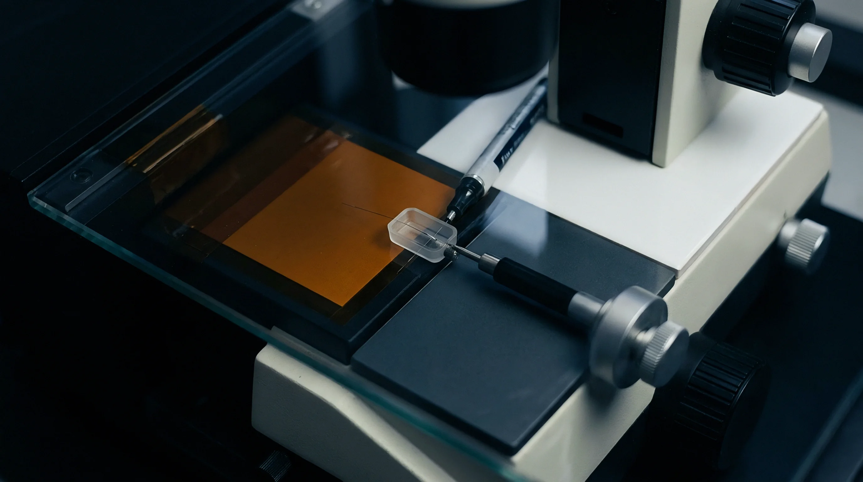
Polymeric adhesives selected for die bonding in inertia sensors operate between mechanical isolation demands and structural stability requirements. High-modulus epoxies offer superior mechanical shear strength and low outgassing characteristics, but transfer excessive package strain directly into the sensor die. Ultra-soft silicone elastomers reduce shear stress transfer by more than 90 percent due to low shear moduli below 5.0 megapascals, yet exhibit high coefficients of thermal expansion and lower resistance to creep under sustained high-g shock events.
Selecting die attach polymers necessitates evaluating material properties above and below the glass transition temperature. Near the glass transition point, polymer elastic modulus drops by up to two orders of magnitude while the thermal expansion coefficient increases by a factor of three. If the glass transition falls within the operational temperature window of the sensor, non-linear changes in mechanical strain transmission render electronic temperature compensation inaccurate.
| Polymer Class | Storage Modulus at 25C (MPa) | Glass Transition Temperature (C) | CTE Below Tg (ppm/C) | CTE Above Tg (ppm/C) | Zero-G Shift (-40C to 125C) |
|---|---|---|---|---|---|
| High-Modulus Conductive Epoxy | 4500 | 145 | 35 | 110 | 1.85 g |
| Low-Modulus Flexible Epoxy | 420 | -15 | 65 | 180 | 0.32 g |
| Silicone Elastomer Gel | 2.5 | -115 | 280 | 310 | 0.04 g |
| Silica-Filled Soft Epoxy | 180 | -35 | 45 | 130 | 0.12 g |
| Polyimide Die Attach Adhesive | 3200 | 220 | 40 | 120 | 1.40 g |

Viscoelastic Behaviour above and below Glass Transition
Modulus variations across temperature regimes govern how much strain transfers from package frames into microelectromechanical elements. Cured epoxies below their glass transition display glassy elastic behaviour, transmitting instantaneous strain with minimal phase lag. Above the glass transition point, rubbery viscoelastic properties introduce time-dependent stress relaxation.
Polymer chains slip slowly under constant applied strain, causing zero-g offset voltage to drift continuously over hours of dwell time at elevated temperatures.
Viscoelastic relaxation degrades long-term stability. Unfilled resins show higher creep rates. When thermal ramps reverse, relaxed polymer networks retain residual strain, creating baseline thermal hysteresis loops.
Formulations engineered for micro-g motion sensors utilize glass transition temperatures situated well outside the operational range, either below minus 50 degrees Celsius using specialized silicone systems or above 175 degrees Celsius using densely cross-linked polyimides.
Viscoelastic stress relaxation in cured epoxy causes time-dependent bias hysteresis following temperature transients.

Filler Particle Loading and Thermal Expansion Characteristics
Silica spheres distributed within an elastomer matrix reduce thermal expansion mismatch while increasing shear stiffness. Modifying polymer formulations through particulate loading alters bulk material performance. Pure silicone matrix material features a coefficient of thermal expansion exceeding 250 parts per million per degree Celsius.
Incorporating 60 to 75 weight percent spherical silica filler drops effective thermal expansion to approximately 50 to 70 parts per million per degree Celsius, while elevating storage modulus from 1.5 megapascals to 150 megapascals.
Distributing particle diameters uniformly avoids stress concentrations along the silicon interface. Filler loading must remain below the percolation threshold where particle-to-particle physical contact turns the matrix rigid. Polymer material selection follows a structured evaluation protocol during design freeze:
- Glass Transition Verification Standardize differential scanning calorimetry to confirm glass transition temperatures lie outside the minus forty to plus one hundred twenty-five degrees Celsius window.
- Modulus Profile Mapping Dynamic mechanical analysis measures storage and loss moduli across operating temperature boundaries at specified vibration frequencies.
- Outgassing Assessment ASTM E595 testing ensures total mass loss remains under one percent and collected volatile condensable material stays below zero point one percent.
- Viscoelastic Drift Auditing Long-term dwell testing under sustained mechanical shear quantifies time-dependent zero-g bias creep rate.
Material vendors frequently explain baseline offset instability by attributing post-cure drift to ambient humidity absorption rather than inherent viscoelastic stress relaxation within the polymer matrix.

Geometry
Bond line pattern architectures define how stress gradients distribute across the lower surface of silicon accelerometer dies. Continuous, full-coverage adhesive layers lock the entire die area to the leadframe, creating maximum shear transfer at die edges. Discontinuous adhesive geometries alter this mechanical constraint.
Confining polymer attachment to central zones leaves die edges free to float above the package substrate without experiencing bending moments generated by leadframe expansion.
Dot array bonding isolates active comb regions. Dispensing five discrete dots, one central anchor plus four small corner stabilization points, reduces transmitted strain energy by over 60 percent compared to full-area coverage. Total adhesive footprint reduction minimizes total thermal shear force transmitted into the silicon bulk.
Can Stepped Curing Profiles Prevent Interfacial Delamination?
Progressive thermal stages allow solvent evaporation and initial cross-linking without inducing localized thermal shock in micro-structures. Solvent entrapment within thick adhesive bonds creates localized gas voids during rapid thermal curing ramps. Interfacial voids alter local compliance, creating asymmetric stress distribution across adjacent sensing comb arrays.
Staged ramping profiles allow volatile components to escape before gelation locks the matrix structure in place.
Thick bond lines absorb mechanical mismatch through shear deformation. Controlling bond line thickness requires adding calibrated spacer beads, typically glass or solid polymer spheres, into the adhesive formulation. A uniform 30-micrometer bond line layer exhibits lower absolute stiffness across its thickness vector than a 10-micrometer bond line layer, dampening leadframe warpage before strain reaches the active silicon substrate.
| Dispensing Pattern Geometry | Coverage Area Ratio (%) | Peak Shear Stress at Die Edge (MPa) | Zero-G Shift (-40C to 125C) | Resonant Frequency Shift (%) |
|---|---|---|---|---|
| Full Area Coverage (Solid) | 100 | 18.4 | 1.25 g | 0.05 |
| 5-Dot Matrix Pattern | 25 | 5.2 | 0.18 g | 0.12 |
| Cross / X-Pattern Dispense | 40 | 8.1 | 0.42 g | 0.08 |
| Peripheral Ring Frame | 30 | 14.1 | 0.98 g | 0.06 |
| Single Center Dot Pedestal | 10 | 1.8 | 0.03 g | 1.85 |
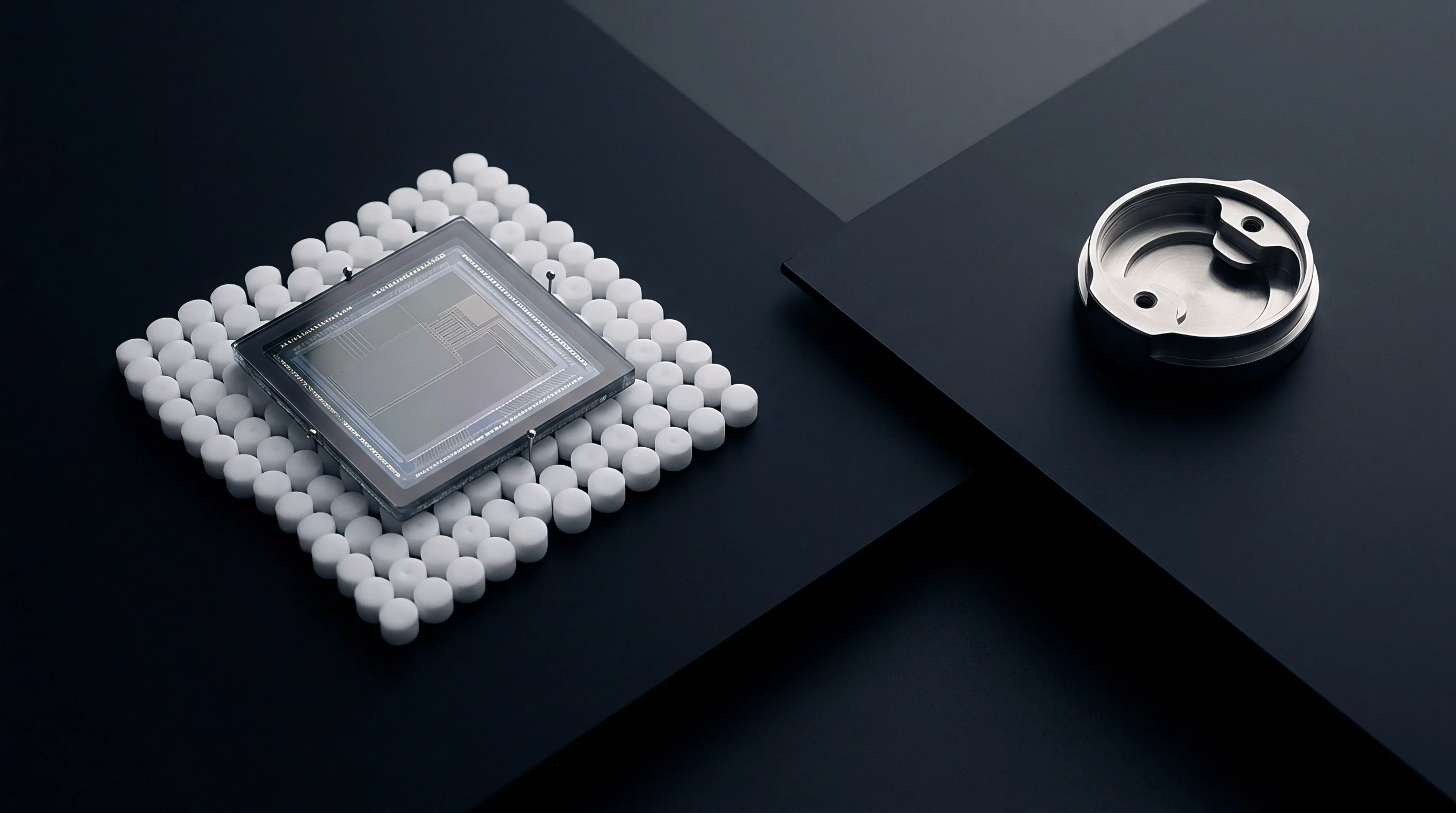
Pedestal Mounts and Center-Point Anchoring Configurations
Isolating suspended proof masses requires minimizing physical contact areas between silicon substrates and organic carriers. Incorporating a micro-machined silicon or glass interposer pedestal between sensor die and package frame isolates active comb regions from bending strain. The pedestal presents a reduced cross-sectional bonding area positioned exclusively under the die center of mass.
To quantify the mechanical isolation effect, take a 2.0-millimeter by 2.0-millimeter capacitive accelerometer die with a nominal thickness of 400 micrometers mounted on a copper leadframe. Assume a baseline sensing gap of 1.200 micrometers yielding a nominal overlap capacitance of 2.000 picofarads. Under a 100-degree Celsius temperature elevation, standard full-area epoxy bonding induces a package-driven radius of curvature equal to 0.85 meters across the silicon substrate.
The physical deflection across the outer 1.0-millimeter die radius calculates as:
w = r^2 / (2 R) = (1.0 x 10^-3 m)^2 / (2 0.85 m) = 5.88 x 10^-7 m = 0.588 micrometers
This warpage tilts the outer stator comb anchors, altering the resting gap differential by 0.042 micrometers on peripheral comb fingers. The resulting change in differential capacitance is:
Delta C = C0 (Delta d / d0) = 2.000 pF (0.042 um / 1.200 um) = 0.070 picofarads
For a sensor with a sensitivity scale factor of 0.100 picofarads per g, this mechanical deformation generates an uncompensated zero-g bias error of 0.700 g. Interposing a central pedestal reducing the attachment radius to 0.20 millimeters reduces edge deflection to 0.023 micrometers and caps the thermal zero-g shift at 0.028 g under identical test conditions.
Glass beads establish uniform bond height. Executing precise die attach dispensing follows a strict physical sequence:
- Substrate thermal pre-conditioning removes surface moisture and stabilizes carrier temperature prior to fluid dispensing.
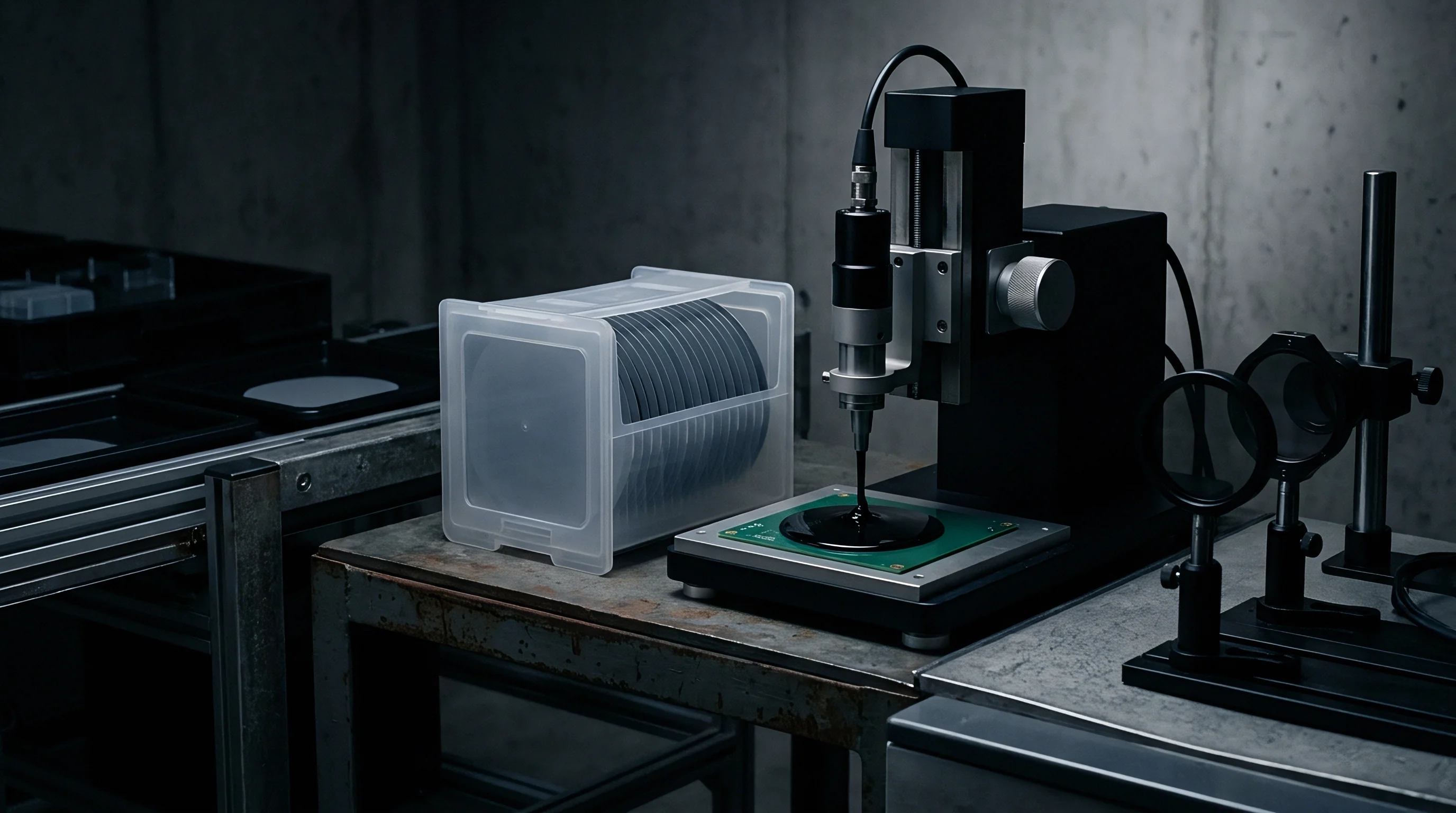
- Volumetric needle dispensing applies controlled polymer micro-dots with automated optical feedback verifying deposit positioning within a plus or minus 15-micrometer tolerance.
- Die pick-and-place tools present the silicon chip, applying controlled placement force between 0.5 and 2.0 newtons to spread adhesive without crushing internal glass spacer beads.
- In-situ optical inspection validates fillet rise along outer chip sidewalls, ensuring epoxy height remains below 50 percent of total die edge thickness.
- Controlled conveyor transit transfers assembled leadframes into cleanroom curing ovens to prevent ambient dust contamination during initial heating.
Dispensing soft adhesive dots at the center of the die minimizes peripheral strain transfer while preserving mechanical anchor integrity.
Keeping adhesive dots positioned inside the central neutral axis of the silicon die minimizes shear coupling to active comb structures.


Bake
Thermal processing profiles during adhesive cross-linking dictate the baseline strain stored within cured polymer networks. Curing polymers at elevated temperatures locks in zero-strain reference conditions at the peak curing point. Cooling the assembled sensor package down to room temperature introduces thermal stress immediately as copper leadframes contract faster than silicon die.
The delta between curing temperature and room temperature defines the intrinsic pre-stress loaded into the sensor prior to operational use.
Over-curing increases modulus and brittleness. Minimizing locked-in assembly stress demands lower curing temperatures extended over longer duration cycles, or room-temperature UV-initiated curing followed by secondary thermal stabilization. Fast cure cycles run at 150 degrees Celsius create residual shear stress states up to three times higher than staged profile curing initialized at 80 degrees Celsius.

Low-Temperature Ramping to Minimize Moisture Entrapment
Volatile release prior to resin vitrification prevents micro-void formation along lower die interfaces. Thermal ramps executed too rapidly boil off residual solvents before cross-linking completes, generating micro-void networks. Acoustic microscopy inspection reveals that interfacial void coverage above 5 percent creates stress concentration points that focus mechanical strain into adjacent silicon regions.
Moisture absorption lowers glass transition point. Uncontrolled atmospheric humidity during storage and pre-bake handling hydrolyzes polymer precursor bonds, altering cross-linking density. Executing die attach baking operations inside nitrogen-purged atmosphere enclosures prevents oxidative degradation of flexible polymer backbones.
| Profile Designation | Ramp Rate (C/min) | Isothermal Hold (C / Time) | Interfacial Void Area (%) | Residual Room-Temp Strain (ue) |
|---|---|---|---|---|
| Rapid Single-Stage Thermal | 10.0 | 150 C / 15 min | 8.2 | 1450 |
| Standard Industrial Ramp | 5.0 | 120 C / 45 min | 3.1 | 920 |
| Staged Low-Temperature Cure | 1.5 | 80 C / 60 min + 120 C / 30 min | 0.4 | 380 |
| UV-Pre-Cure Plus Thermal Ramp | 2.0 | UV 30s + 100 C / 30 min | 0.1 | 210 |
Void percentage directly influences thermal stress concentrations. Documenting polymer qualification procedures requires compiling specific material and process verification parameters into the sourcing lot record:
- Thermal Differential Scanning Calibrations Documentation confirming complete chemical reaction completion with residual exotherm energy below 2.0 joules per gram post-cure.
- Acoustic Microscopy Inspection Logs C-mode scanning acoustic microscopy records proving total interfacial voiding occupies less than 1.0 percent of total bond area.
- Thermogravimetric Analysis Dossiers Weight loss monitoring data showing total volatile release during high-temperature bake stays under 0.2 percent by weight.
- Bond Line Geometry Records Optical cross-section verifications confirming bond line thickness variation across the die area stays within plus or minus 3.0 micrometers.
AEC-Q100 Grade 1 thermal shock testing between minus fifty-five and plus one hundred fifty degrees Celsius rejects die attach formulations showing over three percent void area by acoustic microscopy.
Incorporate AEC-Q100 Grade 1 thermal cycling requirements into procurement specifications to reject die attach lots exhibiting creep-induced offset shifts.
Screening
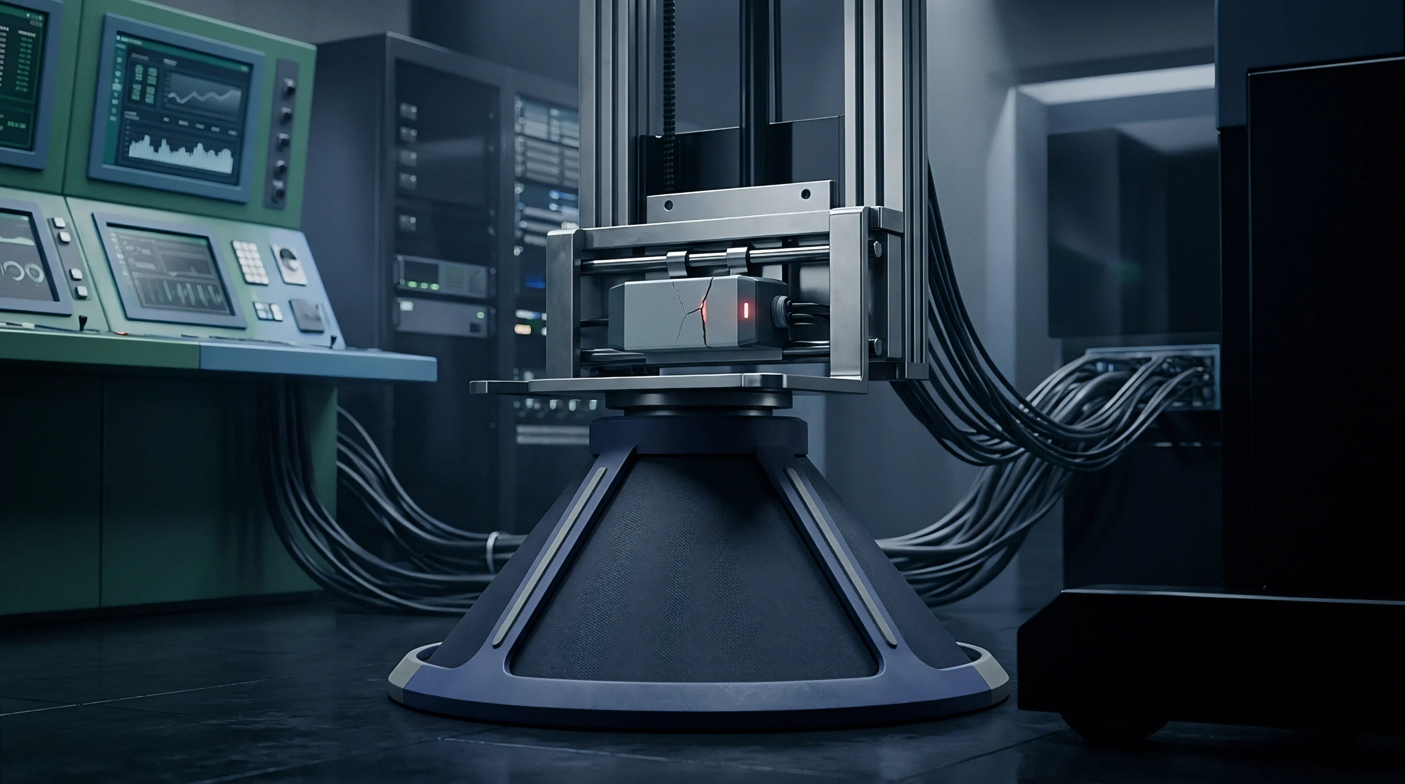
Verifying post-encapsulation zero-g bias stability requires environmental chamber testing across extended thermal sweeps. Accelerometers undergo thermal ramp cycles inside precision environmental chambers while logging continuous offset voltage output. Unmitigated package stress reveals itself as non-repeatable zero-g offset traces during upward and downward temperature sweeps, forming baseline thermal hysteresis loops.
Screening protocols evaluate short-term thermal response alongside long-term viscoelastic relaxation under mechanical pre-stress. Exposing packaged devices to elevated temperature storage at 125 degrees Celsius for 1000 hours accelerates polymer chain creep, allowing quality control audits to detect unstable die attach formulations prior to commercial deployment.

Hysteresis Quantification and Long-Term Bias Drift Measurement
Thermal cycling between lower and upper operating limits reveals non-reversible mechanical offsets in micro-machined capacitive structures. Calculating thermal hysteresis involves subtracting offset values measured at room temperature during an upward thermal swing from values taken at room temperature following cooling from maximum operating temperature. High-precision capacitive accelerometers targeting tactical inertial guidance require thermal hysteresis figures below 0.5 milligrahs across a minus 40 to plus 85 degrees Celsius operating envelope.
Temperature excursions induce zero-g offset drift. When raw mechanical stress mitigation via polymer selection and geometry optimization leaves residual thermal drift, electronic signal conditioning offers secondary compensation. Integrated temperature sensors on the MEMS die monitor real-time thermal state, feeding digital signal processors that compute multi-order polynomial correction curves.
Polymer die attach stress mitigation reduces initial physical non-linearities to a magnitude that polynomial registers can process without saturating dynamic range.
Polyimide adhesives require elevated curing temperatures. Solder attachment yields higher thermal strain. Whether multi-axis capacitive accelerometers can maintain micro-g bias stability over decade-long lifespans without active firmware strain-sensing compensation remains unresolved across high-reliability aerospace applications.