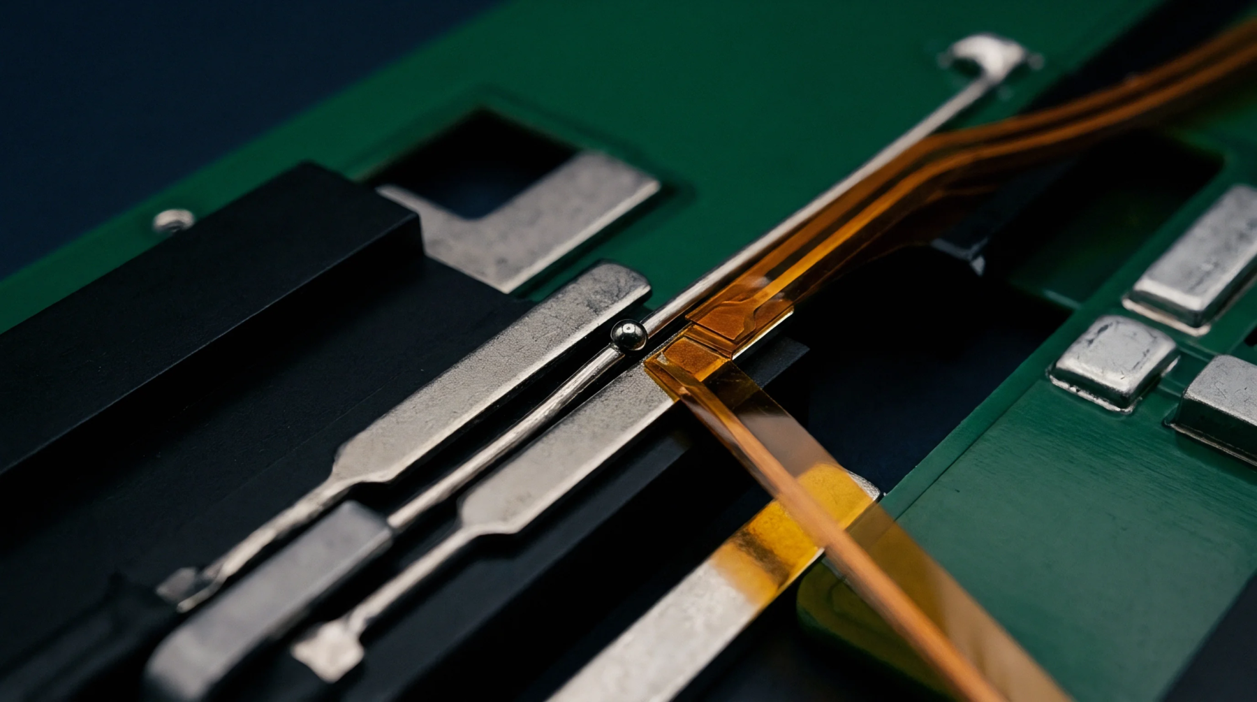
Mechanical Strain
Structural deformation of circuit boards during assembly, testing, or operation causes mechanical stress on mounted components. Severe issues arise from pcb flexure when surface-mount devices like ceramic capacitors or ball grid array packages experience solder joint cracking. This physical bending occurs during panel singulation, connector insertion, or under high vibration.
Measurement Method
Metrological quantification of the board deformation utilizes strain gauges attached directly to the board surface near critical components. Engineers monitor pcb flexure by measuring microstrain during mechanical assembly steps, comparing results against industry standards like IPC-9704A. This process separates benign handling stress from damaging mechanical deflection before final assembly.
Strain Limit
Allowable deflection thresholds are established by component manufacturers and system integrators to prevent internal component damage. These pcb flexure limits depend heavily on board thickness, solder alloy composition, and component package size. Real-time logging of strain ensures that any process exceeding the established tolerance is immediately flagged for adjustment.
Calibration Standard
Verification of the strain measurement system is conducted using high-precision reference cantilever beams with known mechanical loads. Drift in the sensing hardware and temperature interference can erode measurement accuracy, requiring periodic recalibration of the signal conditioning amplifiers. Certification of the test fixture is typically performed annually to guarantee that measured flexure values correspond to actual structural load.
Without this systematic calibration, sensor drift or thermal noise can distort the data, leading to false passes that hide damaging strain events in the production line.