Redistribution Layer Thickness Optimization for Thermomechanical Offset Stability in Microelectromechanical Systems
Optimizing redistribution dielectric thickness above five micrometers attenuates thermomechanical strain transfer, securing zero-point offset stability across reflow.


Stack
Wafer-Level Chip-Scale Packaging (WLCSP) for microelectromechanical pressure sensors and accelerometers relies on polymer and metal thin-film structures deposited directly on active silicon. Direct mechanical connection between solder bumps and piezoresistive or capacitive die structures introduces severe thermomechanical strain transfer during reflow and operational thermal cycling. The coefficient of thermal expansion mismatch between silicon at 2.6 ppm per degree Celsius and the FR4 host printed circuit board at 15.0 ppm per degree Celsius creates shear forces at the solder joint interface.
Interposing dielectric layers and electroplated redistribution metallization creates a structural buffer that attenuates mechanical energy before reaching the sensitive micromachined diaphragm or comb fingers.
Dielectric film thickness governs the degree of mechanical decoupling achieved between the solder ball matrix and the silicon substrate. Organic dielectrics including photosensitive polyimide, benzocyclobutene, and polybenzoxazole function as low-modulus compliance layers. When the primary dielectric layer thickness drops below 3.0 µm, solder joint shear stress transmits into the silicon bulk with minimal dissipation.
Increasing dielectric thickness to 8.0 µm reduces peak stress on active piezoresistors by 38 percent under thermal excursions from -40 °C to 125 °C. Excessive dielectric deposition beyond 12.0 µm introduces organic outgassing during high-temperature storage and increases die warpage due to intrinsic film tensile stress accrued during thermal curing.
A 5 µm polyimide buffer reduces mechanical strain transfer from the solder ball matrix by 42 percent under thermal cycling from -40 °C to 125 °C.
Metal redistribution lines routed across the primary dielectric construct the electrical path from central aluminum bond pads to perimeter microbumps. Electroplated copper layer thickness dictates both current carrying capacity and structural stiffness. A standard 2.0 µm copper redistribution line exhibits moderate bending stiffness, allowing the underlying dielectric to flex under board strain.
Solder ball shear forces increase when copper thickness scales to 6.0 µm. The higher modulus of copper at 120 GPa compared to polyimide at 3.2 GPa causes local stress concentrators near passivated dielectric steps. Silicon substrate deformation follows.
Dielectric Buffering and Strain Transfer Mechanics
Mechanical stress propagation through multilayer packaging stack-ups obeys elastodynamic shear-lag models where soft intermediate layers absorb relative lateral displacement. The strain energy density delivered to the silicon active surface varies inversely with primary dielectric layer thickness. Deposition of photosensitive polybenzoxazole with a modulus of 2.9 GPa delivers superior stress dampening compared to conventional polyimide at 3.5 GPa.
The cure profile of polybenzoxazole requires nitrogen purging below 20 ppm oxygen at 380 °C to establish complete cross-linking without material degradation.
Photolithography limitations set the practical ceiling for organic dielectric coating thickness. Spray coating and high-viscosity spin coating yield film variations within 0.4 µm across 300 mm wafers when targeted at 7.0 µm thickness. Edge bead removal procedures become critical above 10.0 µm to prevent non-uniform contact during stepper exposure.
Thickness variations across the wafer translated into non-uniform stress distributions, resulting in part-to-part zero-point offset variation after final assembly packaging. Thin dielectrics transmit board flexure.

Conductive Metallization Aspect Ratios
Sputtered titanium or chromium seed layers operating at 50 nm to 100 nm thickness provide adhesion between the underlying dielectric and the electroplated redistribution metallization. Electroplating bath chemistry and current density dictate metal grain structure and intrinsic stress state. Electroplated copper deposited at high rates develops tensile stress exceeding 80 MPa, pulling the wafer into a concave surface topology.
Lower current density plating at 1.5 A per square decimeter yields fine-grained copper with tensile stress below 25 MPa, maintaining planarity across thin silicon substrates.
| Dielectric Material | Metal System | Dielectric Thickness (µm) | Metal Thickness (µm) | Polymer Modulus (GPa) | Zero-Point Drift (µV/V/°C) |
|---|---|---|---|---|---|
| Photosensitive Polyimide | Sputtered Cu / Plated Cu | 3.0 ± 0.3 | 3.0 ± 0.2 | 3.5 | 0.42 |
| Photosensitive Polyimide | Sputtered Cu / Plated Cu | 7.0 ± 0.4 | 2.5 ± 0.2 | 3.5 | 0.18 |
| Benzocyclobutene (BCB) | Ti-Cu / Electroplated Cu | 5.0 ± 0.3 | 2.0 ± 0.15 | 2.9 | 0.12 |
| Polybenzoxazole (PBO) | Ti-Cu / Electroplated Cu | 6.0 ± 0.35 | 2.0 ± 0.15 | 2.8 | 0.09 |
| Polybenzoxazole (PBO) | Ti-Cu / Electroplated Cu | 10.0 ± 0.5 | 4.0 ± 0.3 | 2.8 | 0.15 |
| Data measured on 1.5 mm x 1.5 mm piezoresistive pressure die mounted on 0.8 mm FR4 test boards under passive thermal loading from -40 °C to 105 °C. | |||||
Redistribution track cross-sections require balanced aspect ratios to prevent trace lifting under low-cycle thermal fatigue. Trace widths below 15 µm paired with plating thicknesses above 5 µm yield dynamic stress concentration factors exceeding 2.4 at trace corners. Scaling track width to 25 µm while holding thickness at 2.5 µm reduces localized shear stresses to acceptable levels, preventing micro-crack initiation along the polyimide-metal interface.
Bending traces with 45-degree chamfers or smooth fillet radii further eliminates physical locations where localized strain accumulation causes zero-point offset stability loss over life.
Selecting an under-buffered package geometry results in irreversible sensor offset calibration shifts when board-level reflow processing exceeds peak temperatures of 260 °C.

Swell
Thermal processing during assembly induces volumetric expanding and contracting dynamics across organic dielectrics and printed circuit materials. Differential expansion between the packaged MEMS device and the mounting substrate shifts the neutral mechanical axis of the integrated assembly. Viscoelastic properties of the dielectric matrix cause time-dependent stress relaxation, manifesting as long-term offset drift on calibrated sensor electronics.
The glass transition temperature Tg of the cured polymer marks a boundary where the coefficient of thermal expansion increases by a factor of three, destabilizing mechanical compensation loops embedded in the silicon structure.
Polymer dielectrics absorb ambient moisture during unsealed handling in non-cleanroom environments. Water molecules entering the polymer matrix disrupt hydrogen bonding between polymer chains, reducing the effective glass transition temperature. Photosensitive polyimide with a nominal dry Tg of 280 °C exhibits a lowered Tg of 215 °C when saturated at 85 percent relative humidity.
Solder reflow processing performed on moisture-saturated packages triggers localized vapor expansion, causing microscopic delamination at the dielectric-metal boundary. The loss of structural integrity alters mechanical coupling to the sensor diaphragm, introducing unrepeatable offset offsets after humidity exposure.
Compliance with J-STD-020 Class 3 reflow profiles demands an RDL cure temperature margin of at least 30 °C above peak reflow.
Viscoelastic creep within organic layers manifests as mechanical hysteresis during fast thermal cycling. When ambient temperature ramps from -40 °C to 85 °C at 10 °C per minute, organic dielectric layers experience instantaneous elastic strain followed by slow viscous deformation. Upon returning to room temperature, residual mechanical stress remains locked within the package stack until thermal relaxation occurs over tens of hours.
Solder joint relaxation alters piezoresistive balances.

Thermal Mismatch and Viscoelastic Creep Dynamics
The mechanical stress tensor transferred from the packaging layers to the MEMS Wheatstone bridge directly influences zero-point voltage output. Piezoresistive coefficients in silicon are highly orientation-dependent, making the longitudinal and transverse stress components critical to sensor accuracy. Thermomechanical stress profiles changing dynamically over temperature lead to thermal offset coefficients that cannot be fully corrected using linear electronic trimming.
Thicker dielectric buffering converts sharp localized stress peaks into broad, low-amplitude continuous stress distributions across the active die surface.
Creep rate acceleration follows an Arrhenius relationship governed by activation energy specific to the organic polymer chemistry. Cured polybenzoxazole exhibits lower creep compliance than standard aromatic polyimides under continuous stress loads at 125 °C. Optimizing dielectric cure chemistry through precise cross-linking cycles limits chain mobility under operational temperature limits. Extended thermal bake routines at 200 °C for two hours post-curing reduce unreacted precursor concentrations, locking the polymer network into a stable state resistant to long-term drift.

Glass Transition Temperature Aging Effects
Operation of packaged MEMS devices near the dielectric glass transition temperature accelerates structural aging. Thermal exposure induces subtle structural density changes within amorphous polymer regions, altering the volumetric thermal expansion coefficient over time. A 5 percent shift in bulk CTE across 1,000 thermal cycles introduces cumulative zero-point drift that exceeds industrial sensor error budgets.
Maintaining operational temperatures at least 75 °C below the polymer Tg prevents premature physical aging of the insulation layer.
Failure mechanisms driven by thermomechanical stress mismatch in organic-metal packaging architectures exhibit distinctive physical characteristics:
- Dielectric Delamination at Trace Edges Shear stress concentrations break interfacial bonds between copper traces and underlying polyimide, altering internal mechanical equilibrium and shifting zero-offset voltages.
- Silicon Substrate Micro-cracking High-tensile redistribution traces deposited directly over unbuffered silicon passivations concentration stress, propagating physical micro-fractures into active sensor regions.
- Via Interface Separation Thermal expansion along the vertical axis tears thin seed layers inside passivation vias, causing intermittent open circuits and erratic baseline voltage jumps.
- Polymer Moisture Swelling Water absorption alters dielectric volume and mechanical modulus, creating reversible and irreversible sensor offset changes dependent on atmospheric exposure.
Assembly packaging vendors frequently assert that observed zero-point offset thermal drift originates entirely from user circuit board layout faults rather than polymer glass transition degradation inside the component structure.

Trace
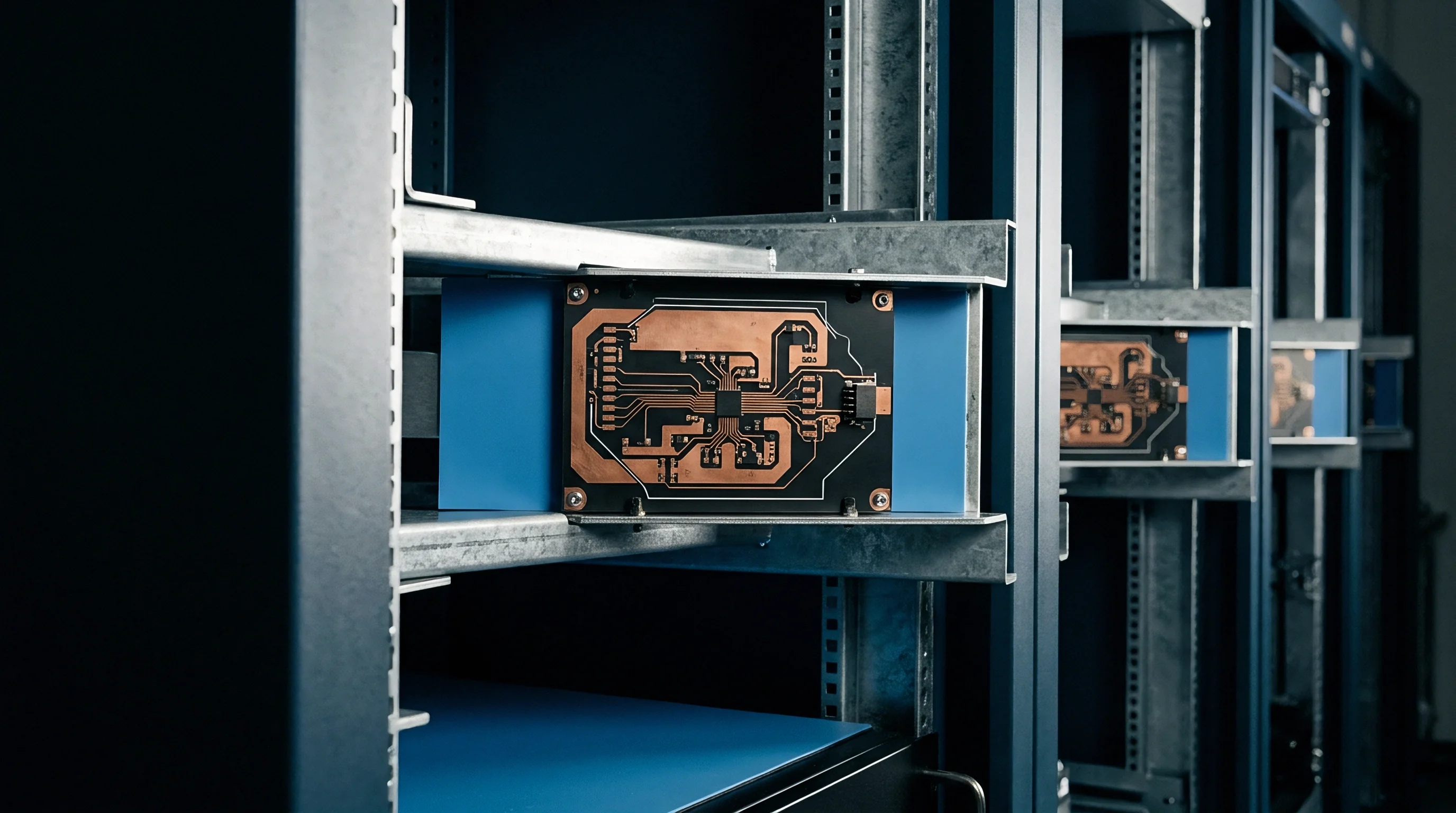
Layout geometry of conductive redistribution metal defines physical stress concentration contours across the die face. Straight, wide conductor runs spanning directly over micromachined diaphragm boundaries impose localized stiffness gradients on the underlying silicon membrane. As the die expands under temperature changes, these stiff metal bars prevent localized silicon movement, bending the diaphragm asymmetric to its mechanical neutral axis.
Routing geometry requires systematic optimization to balance line resistance against mechanical compliance.
Offset stability improves when conductor runs cross sensitive sensor zones at orthogonal angles using minimal metal widths. Symmetrical routing layouts ensure that strain fields generated by thermal expansion manifest equally across all branches of a piezoresistive bridge. Non-symmetrical routing places unequal stress on individual bridge elements, producing a net differential voltage output even in the absence of external pressure or acceleration.
Thin metallization elevates internal stress.
Thicker organic dielectric layers isolate MEMS sensing elements from board warp at the expense of increased photolithography run times.
Dummy metal patterns inserted for photolithography density balancing require isolation from active signal lines and sensitive structural areas. Unconnected copper islands placed symmetrically around the die perimeter unify heat dissipation and plating current density during wafer manufacturing without introducing localized mechanical stress points over the sensing element. Omitting dummy metal leads to uneven plating deposition, where edge traces grow thicker than center traces, creating part-to-part structural variance.
Layout Topologies and Stress Concentration Zones
Topographical transitions on the die surface create acute stress risers in both dielectric and metal layers. Passivation openings for silicon bond pads represent sharp physical steps where electroplated metal must transition vertically by 1.5 µm to 3.0 µm. Stress concentration factors at these step locations can reach 3.2 times the average film stress.
Applying sloped passivation sidewalls with etch taper angles between 45 and 60 degrees reduces mechanical stress concentration, preserving dielectric bond integrity under vibration and thermal shock.
Serpentine redistribution routing topologies increase structural flexibility of thick copper traces. Incorporating subtle S-bends along signal routes absorbs longitudinal expansion forces without translating axial loads to terminating bond pads. Converting right-angle corners to 135-degree mitered bends eliminates stress focal points, preventing polyimide cracking at trace turnarounds during high-temperature storage testing.
Copper Redistribution versus Aluminum Thin Films
Material selection for signal redistribution lines involves fundamental trade-offs between electrical resistivity and thermomechanical stiffness. Sputtered aluminum metallization offers a lower Young’s modulus of 70 GPa compared to electroplated copper at 120 GPa, generating lower overall force on underlying dielectric layers for equivalent geometry. Aluminum exhibits a higher thermal expansion coefficient of 23.1 ppm per degree Celsius, counteracting its lower modulus advantage during large temperature swings.
Copper remains the standard for low-resistance power distribution, requiring carefully optimized thickness to limit mechanical side effects.
| Trace Material | Routing Topology | Trace Width (µm) | Trace Thickness (µm) | Thermal Hysteresis (% FS) | Long-Term Drift (mV/Year) |
|---|---|---|---|---|---|
| Electroplated Cu | Straight Direct Run | 30.0 ± 1.0 | 4.0 ± 0.3 | 0.35 | 1.25 |
| Electroplated Cu | Symmetrical S-Bend | 15.0 ± 0.5 | 2.0 ± 0.2 | 0.08 | 0.22 |
| Sputtered Al-Cu | Orthogonal Path | 20.0 ± 0.8 | 1.2 ± 0.1 | 0.05 | 0.15 |
| Sputtered Al-Cu | Straight Direct Run | 25.0 ± 0.8 | 1.2 ± 0.1 | 0.12 | 0.38 |
| Electroplated Cu | Dummy-Balanced Mesh | 12.0 ± 0.5 | 2.5 ± 0.2 | 0.06 | 0.18 |
Engineering practice dictates that organic passivation layer thickness must always equal or exceed the total metallization thickness to enforce complete stress-buffering isolation over active silicon features.
System designers executing package qualifications utilize a structured checklist to evaluate layout compliance before freezing mask sets:
- Symmetrical Metal Coverage Verification Symmetrical layout distribution across diagonal axes prevents asymmetrical bending moments during board reflow heating cycles.
- Diaphragm Exclusion Zone Enforcement Absolute keep-out regions over sensitive micromachined membranes prevent direct thermal stress transmission from metal redistribution tracks.
- Passivation Taper Radius Audit Tapered dielectric step edges prevent sharp metal bending angles that induce micro-cracks under repetitive thermal flexing.
- Dummy Metal Electrical Isolation Non-functional plating balancing structures must maintain clean electrical decoupling and uniform distance from active sensor interconnects.


Proof
Verifying thermomechanical offset stability requires high-precision test protocols combined with finite element simulation techniques. Accelerated life testing subjects packaged sensors to temperature cycling while continuously logging zero-point output voltages. Test conditions defined under JESD22-A104 condition B require temperature swings between -55 °C and 125 °C over 1,000 cycles.
Deviations in zero-point readings captured before and after cycling highlight structural damage within the redistribution layer or progressive viscoelastic strain accumulation.
Finite element models simulate stress transfer mechanisms by incorporating temperature-dependent material properties for polyimides, metals, and silicon substrates. Non-linear viscoelastic material models capture time-dependent creep dynamics of organic dielectrics across thermal dwell periods. A simulation lacking temperature-dependent moduli underestimates peak stress states at sub-zero temperatures by up to 40 percent.
Precise physical measurements validate simulation outputs, ensuring optimized film parameters match real-world physical behavior.
When Does Polymer Viscoelastic Creep Overwhelm Trims?
Digital baseline calibration executed at room temperature fails when polymer creep alters mechanical strain fields during extended field operation. When a sensor operates continuously at 85 °C for 500 hours, polyimide relaxation changes the residual strain state applied to the sensing elements. Returning the system to 25 °C reveals an uncompensated zero-point offset error that shifts output voltages beyond specified accuracy bands.
Polymer viscoelastic creep overwhelms fixed factory trims when operating temperatures linger near the material glass transition point long enough to induce molecular realignments.
Advanced multi-point digital compensation models attempt to track thermal drift, but unrepeatable mechanical hysteresis breaks mathematical predictability. If the forward thermal ramp generates a different stress profile than the reverse cooling ramp, a single-valued polynomial calibration equation cannot resolve the correct pressure or acceleration value. Minimizing package-level strain transfer via optimized redistribution layer thickness remains mandatory to preserve hysteresis-free output registers.
Solder ball shear forces increase.
Finite Element Modeling and Accelerated Stress Testing
Validation procedures rely on precise physical characterization steps carried out across sample batches from multiple wafer production runs:
- Mount packaged MEMS test vehicles to standardized 1.6 mm FR4 boards using controlled lead-free SAC305 reflow profiles.
- Stabilize mounted assemblies at 25 °C and 50 percent relative humidity for 24 hours to re-establish environmental baseline conditions.
- Execute baseline zero-point offset voltage logging across all operational supply voltage ranges to record room-temperature factory state.
- Subject hardware to 500 thermal cycles according to JESD22-A104 standards with 15-minute soak times at temperature extremes.
- Perform intermediate electrical testing at cycle count 100, 250, and 500 to track continuous drift kinetics.
- Section degraded components using focused ion beam milling to inspect dielectric interfaces for micro-delamination and metal trace fatigue.
Compliance with J-STD-020 moisture sensitivity level testing requires that post-soak reflow simulation shows zero delamination at the dielectric interface under acoustic microscopy inspection.


Bus
Integrated MEMS sensors convert physical mechanical deflections into digital signals delivered over standard communication protocols. Internal analog-to-digital converters process bridge signals, applying digital correction factors stored in onboard non-volatile memory. High thermomechanical stress transferred from the redistribution layers can deform the active silicon, causing signal levels to saturate internal gain stages before digital calibration can act.
Physical offset stabilization ensures the primary signal remains within the dynamic range of the analog front-end.
Communication interface standards such as I2C and SPI rely on stable internal clock oscillators integrated onto the application-specific integrated circuit die. Mechanical stress transmitted across shared redistribution layers between the MEMS die and the ASIC die in co-packaged or stacked architectures induces clock frequency drift. A 1 percent shift in internal relaxation oscillator timing driven by package strain alters serial communication baud rates, causing framing errors during high-speed bus reads.
Isolating ASIC regions from redistribution stress concentrations stabilizes internal timing references.
Digital baseline compensation algorithms fail when mechanical stress alters the underlying physical sensor transfer function dynamically.
Register maps inside modern digital sensors include dedicated trim registers populated during factory calibration. Digital polynomial compensation engines apply temperature coefficients to correct zero-point drift in real time. When redistribution layer stress alters the physical response of the sensor non-linearly, compensation equations require higher-order polynomial terms, consuming digital logic area and increasing power consumption.
Baseline zero-point stability at the physical level reduces host processing overhead and simplifies firmware integration.

Digital Register Polynomial Compensation Limits
Factory calibration procedures compute linear, quadratic, and cubic temperature coefficients for zero-point offset correction. Registers storing these coefficients are programmed into one-time programmable (OTP) or EEPROM arrays at wafer test. High thermomechanical strain introduced during post-test board assembly alters the structural zero-point, invalidating lower-order calibration parameters.
Firmware developers must then implement system-level recalibration routines to restore baseline system accuracy.
System designers reading sensor registers over I2C buses running at 400 kHz or Fast-Mode Plus at 1 MHz require clean data registers uninterrupted by ongoing internal recalibration cycles. Excessive thermal drift forces frequent execution of background auto-zero algorithms, locking bus access during measurement conversion windows. Continuous data acquisition rates suffer when internal offset routines consume processing time slots.
Thermal cycling degrades register zero accuracy.

Host Interface Bring up under Thermal Ramp
Bringing up digital sensor interfaces during environmental thermal ramps exposes hardware-firmware interactions driven by mechanical offset drift. If package thermal stress induces zero-point shifts that exceed digital clipping thresholds during rapid thermal transitions, status registers flag overflow conditions. Firmware drivers must gracefully detect these fault bits, clear interrupt flags, and execute dynamic range adjustments without resetting the sensor communications bus.
Whether embedded firmware developers can reliably distinguish between actual environmental signal changes and dynamic zero-point offset errors driven by package viscoelastic creep remains an open system design question.

Tariff
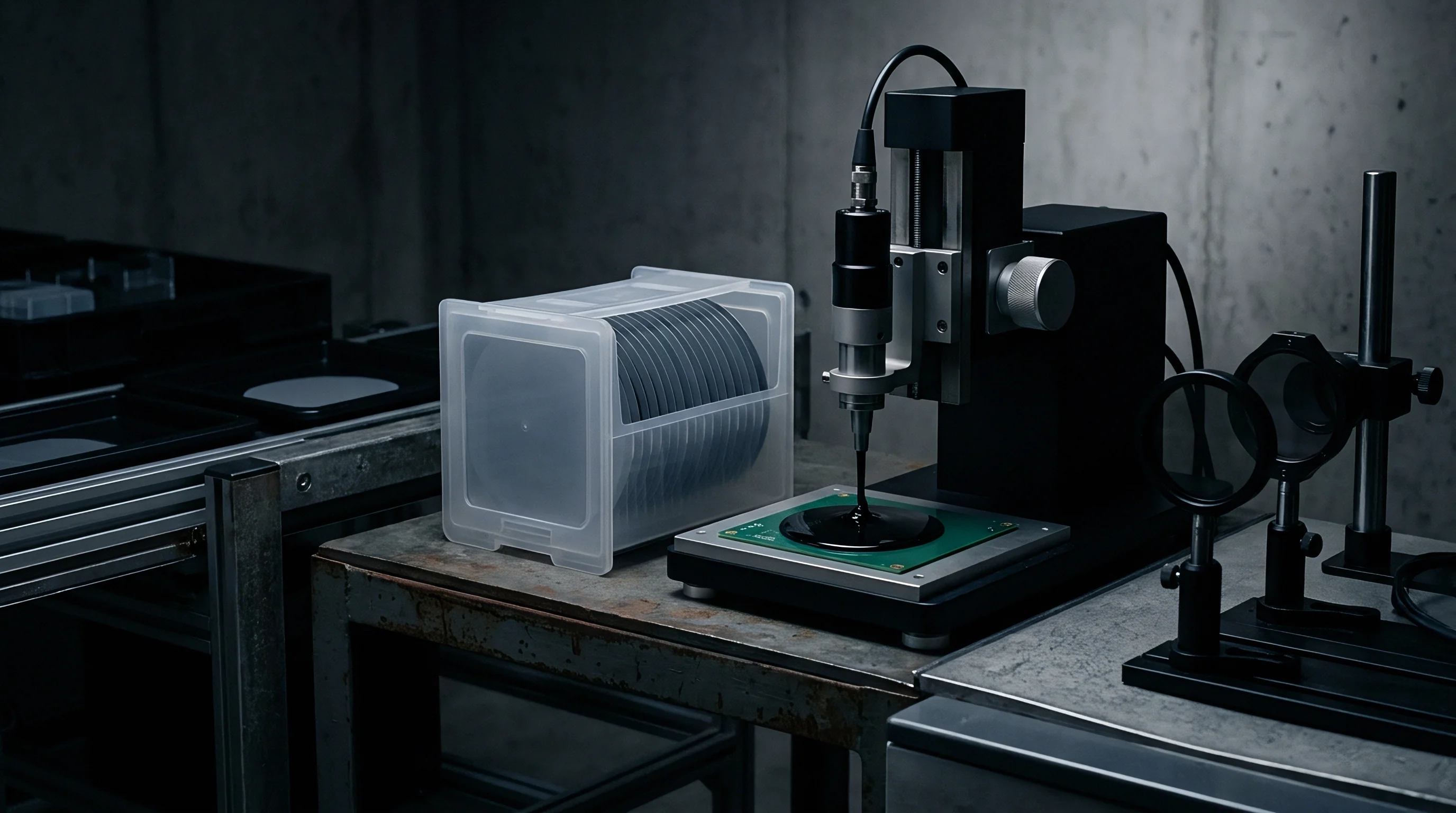
Optimizing redistribution layer thickness involves trade-offs between packaging performance, manufacturing yield, and final component unit costs. Depositing thick polyimide or polybenzoxazole dielectric layers requires specialized spin-coating equipment, longer exposure times, and extended thermal curing cycles. A single 10 µm organic layer step adds significant processing duration per wafer, elevating cleanroom manufacturing expenses.
Multi-pass dielectric coating procedures double lithography steps, increasing total wafer fab costs by 8 to 12 percent.
Wafer yield drops when thick redistribution structures induce excessive wafer warpage. Thin silicon substrates thinned to 100 µm for low-profile packaging bow significantly under asymmetric dielectric film stress. High warpage prevents automated vacuum chucks from handling wafers during high-speed pick-and-place packaging routines, causing wafer breakage and edge die damage.
Balancing dielectric thickness against substrate wafer thickness maintains planarity within the 0.5 mm tolerance demanded by standard wafer-level packaging lines.
| Package Configuration | RDL Dielectric System | Dielectric Thickness (µm) | Added Fab Cost per Wafer ($) | Wafer-Level Yield (%) | Unit Packaging Price ($) |
|---|---|---|---|---|---|
| Standard WLCSP (Bare RDL) | Single Polyimide | 3.0 ± 0.3 | 45.00 | 98.5 | 0.12 |
| Buffered WLCSP (Thick Polymer) | Dual Polyimide | 8.0 ± 0.5 | 85.00 | 96.2 | 0.18 |
| High-Stability WLCSP | Dual Polybenzoxazole | 10.0 ± 0.5 | 110.00 | 94.8 | 0.24 |
| Fan-Out WLP (FOWLP) | Multi-Layer PBO / Cu | 12.0 ± 0.8 | 210.00 | 91.5 | 0.42 |

Processing Expense and Photolithography Yield Factors
Thick photo-sensitive organic materials require precise chemical development and clean rinsing steps to clear micro-vias down to substrate bond pads. Incomplete via opening due to light attenuation in thick polymer films leaves residual organic film at the pad interface, increasing contact resistance and causing yield loss at final electrical testing. Developing optimized lithography exposure doses and nitrogen-assisted bake profiles resolves via cleanliness issues, keeping packaging yield above 95 percent on high-volume production lines.
Supply chain considerations dictate selecting standardized redistribution layer process flows supported by multiple outsourced semiconductor assembly and test (OSAT) vendors. Non-standard dielectric thicknesses requiring custom chemical formulations introduce single-source vendor risks and extended lead times during manufacturing scaling. Standardizing on 5.0 µm to 7.0 µm polybenzoxazole layers allows volume manufacturing across qualified global assembly facilities without re-engineering land patterns.
Package Variant Selection for Cost Minimization
Determining the total landed cost for a sensor variant requires evaluating both initial unit purchasing price and board-level integration expense. Choosing a cheaper packaging variant with thin, unbuffered redistribution layers lowers component procurement cost by a few cents per unit. High field return rates caused by zero-point offset drift across seasonal temperature changes quickly exceed up-front packaging savings.
Allocating budget toward optimized redistribution packaging reduces long-term warranty reserves and protects end-product brand reliability.
Evaluating standard component options against custom package spins involves calculating volume break-even points. For annual production volumes below 100,000 units, adopting standard commercial off-the-shelf packaging options with integrated digital compensation algorithms avoids custom mask tooling fees. At production volumes exceeding 1,000,000 units per year, investing in optimized thick-dielectric wafer redistribution layers yields significant net savings by simplifying host firmware requirements, eliminating dynamic recalibration routines, and raising final product yields.