PCB Substrate Strain Isolation Slot Routing Precision Reference Sourcing
Milling perimeter strain isolation slots with a 1.0 mm bit and 0.35 mm copper keepout attenuates board flexure stress on precision references by up to 24 dB.
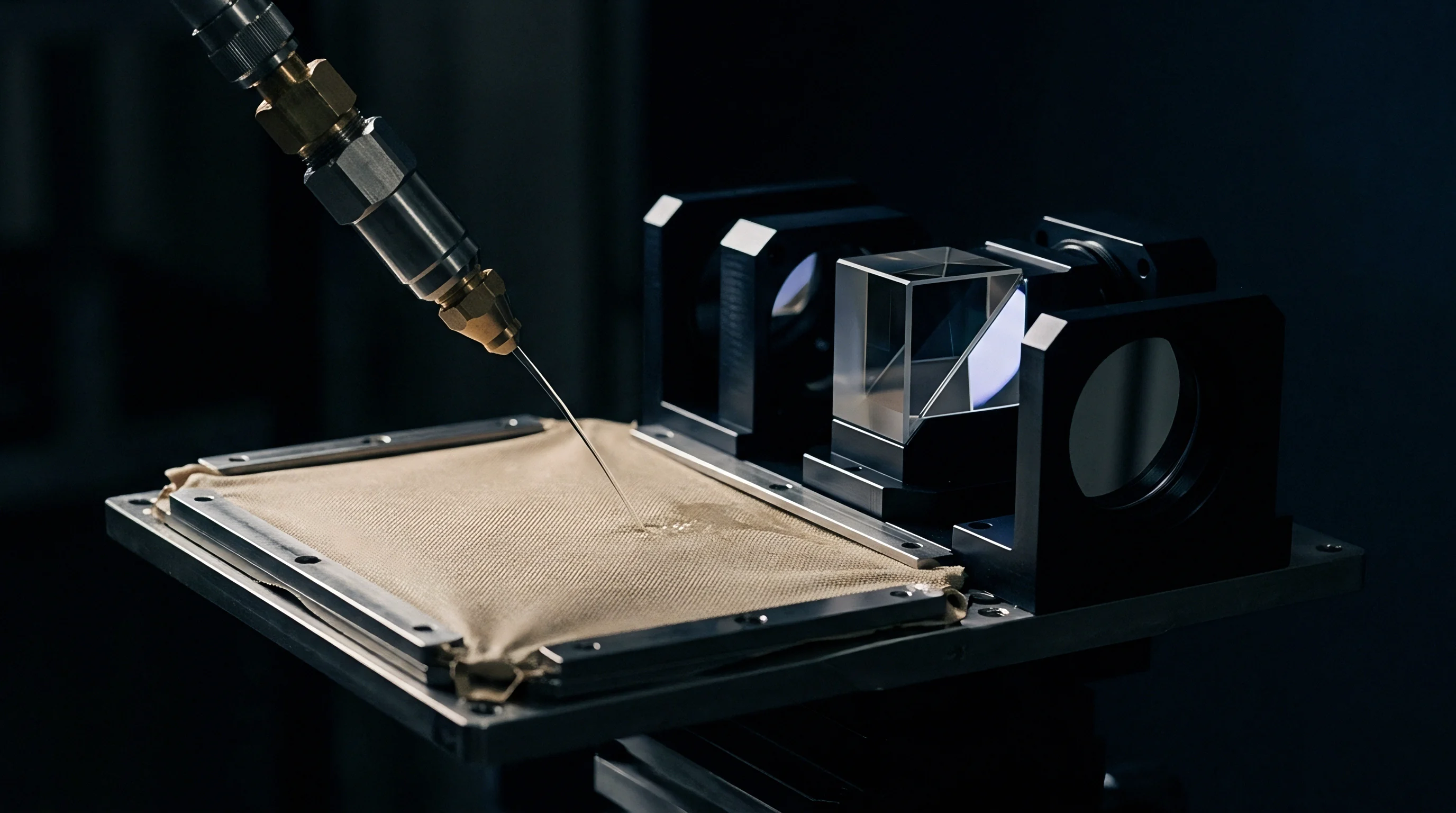

Relief
Precision voltage references and silicon MEMS pressure sensors drift when mechanical stress transfers from the circuit board into the semiconductor package. Substrate isolation slots sever these stress paths by routing open channels through the laminate directly surrounding the sensitive footprint. Milling a U-shaped or perimeter slot isolates the component on a cantilevered tongue or floating substrate island, converting rigid PCB flexure into structural deflection of the peripheral board area.
Solder reflow leaves permanent residual shear stress in surface-mount joint arrays as copper and epoxy cool at different rates than silicon.
Maintaining long-term output stability in a 16-bit or 24-bit measurement circuit requires quantifying the attenuation delivered by slot geometry. Testing under a three-point bend setup demonstrates that a dual 1.2 mm wide routed slot configuration attenuates board-level strain at the IC pads by 18 dB to 24 dB compared to a solid laminate layout. Router bit width determines the mechanical boundary: a 1.0 mm router bit with a ±0.05 mm positional tolerance achieves sufficient compliance without excessively sacrificing board surface area.
A copper-to-milled-edge keepout of 0.35 mm prevents copper exposed along the inner channel wall from shorting or delaminating during high-speed routing operations.

Milled Slot Geometry and Stress Attenuation
How a slot is oriented relative to the primary strain vector directly governs its mechanical isolation efficiency. Circuit boards subjected to chassis mounting torque experience directional strain along defined axes. Positioning long perimeter slots parallel to these strain vectors leaves the component vulnerable to torsional twisting.
Curved slot corners with a minimum inner radius of 0.60 mm prevent stress concentration points at the slot terminations, where micro-cracks form during mechanical shock. A continuous perimeter cut interrupted only by narrow structural ribs provides maximum mechanical decoupling while keeping the component mounted during assembly handling.
A dual-slot isolate pattern reduces board-level mechanical strain on plastic surface-mount IC packages by 72 percent under a three-point bend condition.
Standard surface-mount land patterns require modifications when placed on an isolated substrate tongue. Thermal relief on ground planes connected to the isolated pad array must be adjusted, as reduced copper area limits heat sinking during solder reflow. The thermal mass of an isolated tongue heats faster than the main board, accelerating solder paste wetting and altering the ideal reflow time-above-liquidus profile.
Reducing the peak reflow temperature by 5 °C or shortening the time above liquidus by 8 seconds prevents package deformation on thin, isolated laminate islands.
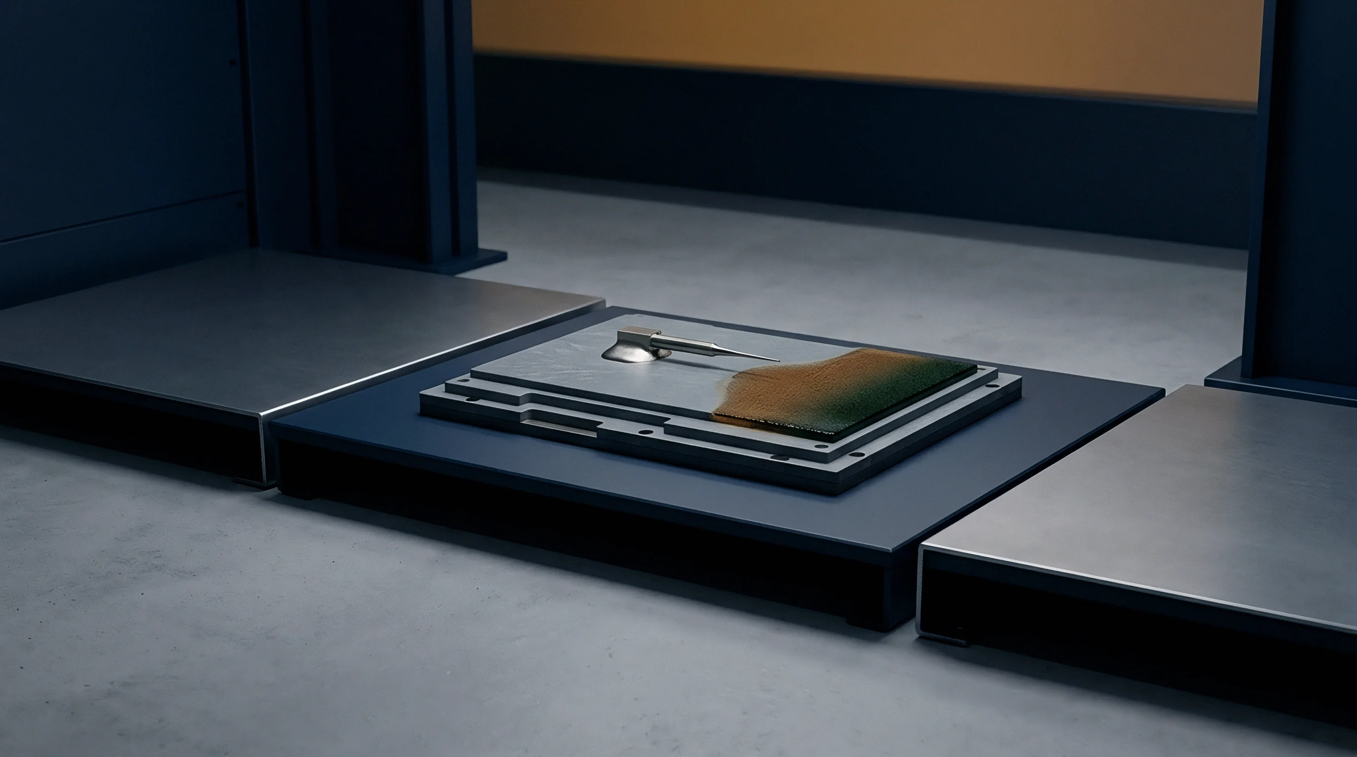
Substrate Keepout Rules for Routed Perimeter Edges
Etched copper features running adjacent to a routed slot suffer from mechanical burrs and edge lifting if positioned too close to the milling path. Gerber drawings must explicitly define the routed slot centerline alongside a dedicated mechanical keepout layer. Standard mechanical tolerances require a minimum distance of 0.30 mm from the outer edge of any copper trace or poured plane to the finished slot perimeter.
Internal ground planes on multilayer boards require an identical pullback distance to eliminate the risk of shorting inner layers through copper dragging during bit pass-through.
Unplated routed slots leave raw fiberglass edges exposed to environmental atmospheric conditions. Epoxy laminates absorb moisture through these freshly cut glass fiber ends, causing localized expansion and subtle dielectric changes near sensitive high-impedance traces. Applying a solder mask dam that overlaps the slot edge by 0.10 mm seals the exposed laminate interface without adding mechanical stiffness across the isolation channel.
Design specifications require verifying whether the panel fabrication shop uses a single-pass end mill or a two-pass plunge cut, as tool engagement speeds directly dictate edge roughness and micro-fracture depth along the slot boundary. What degree of moisture absorption occurs along unplated routed edges over 1,000 hours of temperature-humidity bias testing?

Deflection
Semiconductor piezoresistive behavior converts substrate bending directly into electrical offset error. High-precision buried Zener and bandgap voltage references experience output voltage shifts up to 0.05 percent when exposed to mechanical strain exceeding 500 microstrain. Thermal expansion mismatch between FR4 substrates, which possess a coefficient of thermal expansion near 14 ppm/°C to 17 ppm/°C, and silicon die material, operating near 2.6 ppm/°C, creates sustained mechanical pressure across solder joints over wide operating temperature ranges.
Unanchored substrate islands shift mechanical compliance from the solder joints to the laminate bridge.
Substrate deformation alters die symmetry and trace resistance, shifting calibration constants stored during factory test. Pressure sensors utilizing MEMS diaphragms suffer zero-point output shifts when mounting screw torque twists the PCB frame. Integrating strain isolation slots isolates the package die frame from board-level mechanical bending, maintaining sensor accuracy across assembly operations and operating temperature swings.

Piezojunction Effects in Precision Voltage Standards
Integrated circuit strain sensitivity stems primarily from the piezoresistive property of silicon, where crystal lattice deformation alters majority carrier mobility. Bandgap reference circuits rely on matched PNP or NPN transistor pairs whose base-emitter voltage differentials change under anisotropic physical stress. Plastic mold compound transfers board-level flexure directly into the encapsulated silicon die, generating non-linear drift that onboard digital calibration algorithms cannot distinguish from temperature changes.
Ceramic surface-mount packages reduce mold compound stress transfer, but substrate flexure still propagates through solder joints into the package substrate base.
| Topology Name | Strain Attenuation (%) | Area Penalty (%) | Moisture Path Length (mm) | Singulation Yield (%) |
|---|---|---|---|---|
| Dual Longitudinal Slots | 68 ±3 | 8.2 | 12.5 | 99.4 |
| C-Shaped Perimeter Cut | 84 ±2 | 14.1 | 8.0 | 98.1 |
| Spiral Decoupled Island | 93 ±1 | 22.5 | 4.2 | 94.8 |
| Four-Corner L-Slots | 52 ±4 | 6.0 | 18.0 | 99.7 |
Slot geometry dictates the mechanical transfer function between the outer printed circuit board and the inner isolated island. Spiral decoupled configurations deliver superior strain isolation by extending the physical length of the compliance arm, though they demand significant surface area penalty and increase trace routing complexity. Simple dual longitudinal slots balance mechanical isolation with structural integrity, offering an ideal compromise for compact automotive and industrial sensor assemblies.
Thermal Cycling Stress Propagation across FR4 Laminates
Thermal gradients across printed circuit board assemblies induce localized bending moments due to differential thermal expansion between copper layers and dielectric glass substrate matrixes. During thermal shock testing from -40 °C to +125 °C, un-isolated surface-mount references exhibit output excursions exceeding 35 ppm due to board-level strain alone. Introducing perimeter routing isolation drops thermal-strain induced drift below 8 ppm across the identical temperature cycle.
Isolating precision analog silicon on an unanchored substrate tongue shifts mechanical compliance from the solder joints to the FR4 bridge.
Laminate Tg, or glass transition temperature, directly impacts strain transfer behavior at elevated operating temperatures. Below Tg, FR4 maintains a high flexural modulus near 24 GPa, effectively transferring mechanical forces across the board into component leads. Above Tg, the laminate matrix softens, reducing flexural modulus down to approximately 2 GPa while dramatically increasing z-axis thermal expansion.
Specifying high-Tg FR4 material with Tg exceeding 170 °C ensures consistent mechanical isolation performance across broad operating temperature regimes. Designing isolation slots on boards with low-Tg substrate materials leads to variable strain relief effectiveness as ambient temperatures cross the glass transition threshold. Strain isolation performance improves when the PCB mechanical compliance remains predictable throughout the operating envelope.


Bridge
Structural support tabs retain the isolated PCB island within the main board frame during component placement, reflow soldering, and automated optical inspection. Mechanical depanelization breaks these temporary bridges, releasing the island to float independently within its routed perimeter cut. Bridge design requires balancing sufficient structural stiffness during high-speed surface-mount assembly against low breakaway force during singulation to prevent transferring mechanical shock back into the precision IC.
Breakaway tab design utilizes either perforation holes, commonly termed mouse bites, or solid routed bridges cut with V-grooves. Mouse bite arrays consisting of 0.50 mm diameter plated holes spaced on 0.80 mm centers yield predictable break lines, but leave sharp glass-fiber burrs that project into the routed channel space. Solid routed bridges singulated with a secondary milling cutter deliver clean edges, but introduce significant mechanical vibration into the circuit assembly during the final cutting process.
- Vacuum clean the panel surface to clear conductive debris generated during initial slot milling.
- Inspect routed channel dimensions using optical coordinate measurement tools to confirm width within ±0.05 mm tolerances.
- Apply protective tape or mask over sensitive optical or diaphragm apertures before mechanical depanelization operations.
- Depanel the isolated substrate island using a dual-spindle nibbler or precision router to minimize shock transfer.
- Perform high-magnification edge inspection to verify trace integrity across support bridges and confirm zero copper burrs.
Tab Width and Depanelization Shear Mechanics
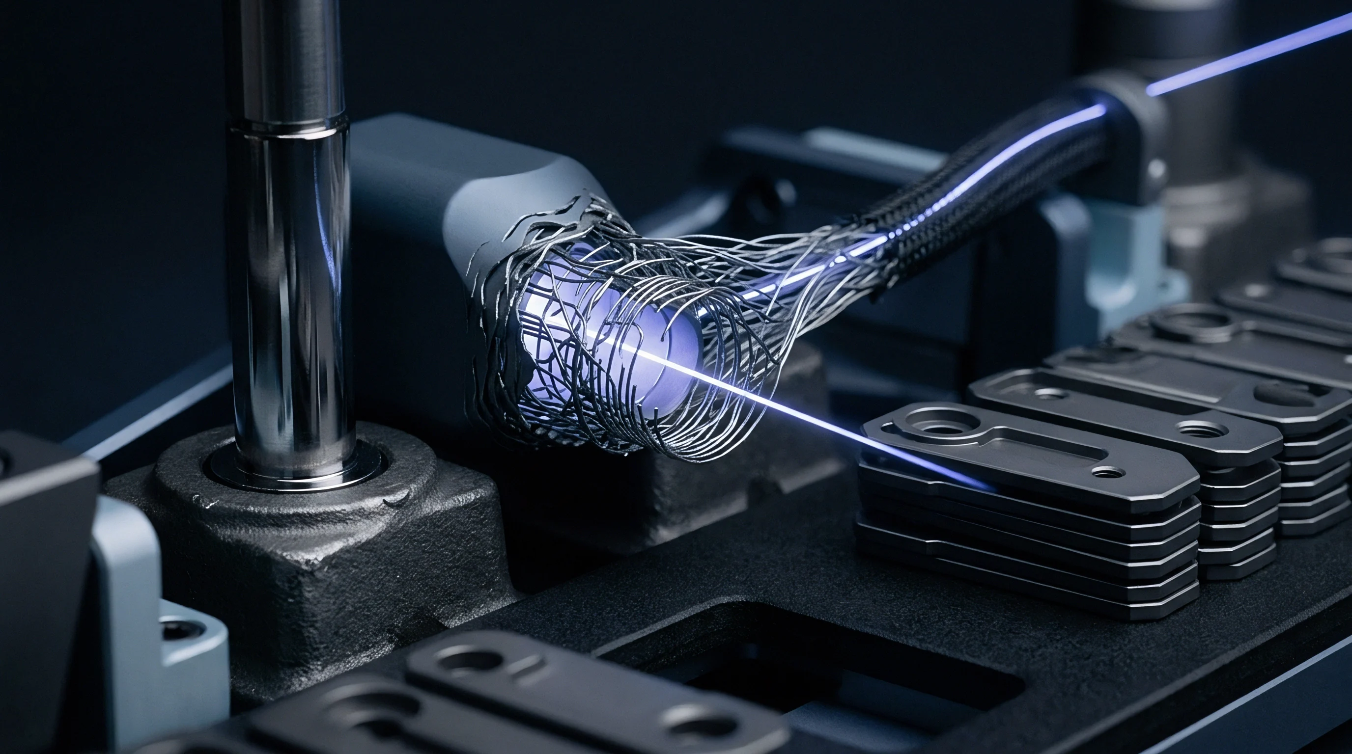
Mechanical shock during depanelization poses severe risks to brittle internal silicon structures and delicate wire bonds within packaged references. Standard punch depanelization exerts shear stress levels exceeding 80 MPa along the break line, transmitting high-frequency vibration spikes directly through the substrate rib into the isolated component land pattern. Laser depanelization completely eliminates mechanical shear stress during singulation, though thermal heat-affected zones must be kept clear of sensitive circuit traces.
Compliance with IPC 2221A routing clearance mandates a minimum distance of half the substrate thickness between plated copper traces and milled slot edges to prevent delamination during depanelization.
Solid bridge width selection dictates the force required for depanelization. A bridge width of 1.0 mm in standard 1.6 mm thick FR4 substrate withstands up to 120 N of lateral force during high-speed surface-mount component placement. Reducing bridge width down to 0.60 mm lowers the required singulation breakaway force by half, but introduces structural deflection risks when heavy placement heads mount components onto the isolated island.
Tooling pins positioned directly under the isolated island during component placement provide physical support, allowing designers to utilize narrower support ribs without risking substrate fracture during SMT processing.

Contamination Control in Milled Perimeter Channels
Milling fiberglass substrate material generates conductive, highly abrasive FR4 dust particles that accumulate inside routed perimeter channels. Un-removed cutting debris trapped within isolation slots bridges the air gap, restoring mechanical coupling across the isolation boundary and degrading low-current electrical insulation. Vacuum extraction systems integrated directly onto CNC router spindles remove the bulk of airborne dust, but electrostatic charge causes fine particles to adhere stubbornly to substrate walls and component bodies.
Conformal coating operations performed after depanelization present significant process control hazards for strain-isolated substrates. Liquid conformal coatings wick into open isolation slots via capillary action, forming a solid polymer bridge across the air gap upon curing. This cured coating bridge restores mechanical stress propagation pathways, negating the strain relief provided by substrate routing.
Masking routed channels with gel dams or applying non-wetting fluoropolymer coatings around slot perimeters prevents capillary bridging, preserving mechanical isolation integrity. Failure to control conformal coating flow across substrate isolation channels results in immediate return of strain-induced output drift following environmental encapsulation.


Bus
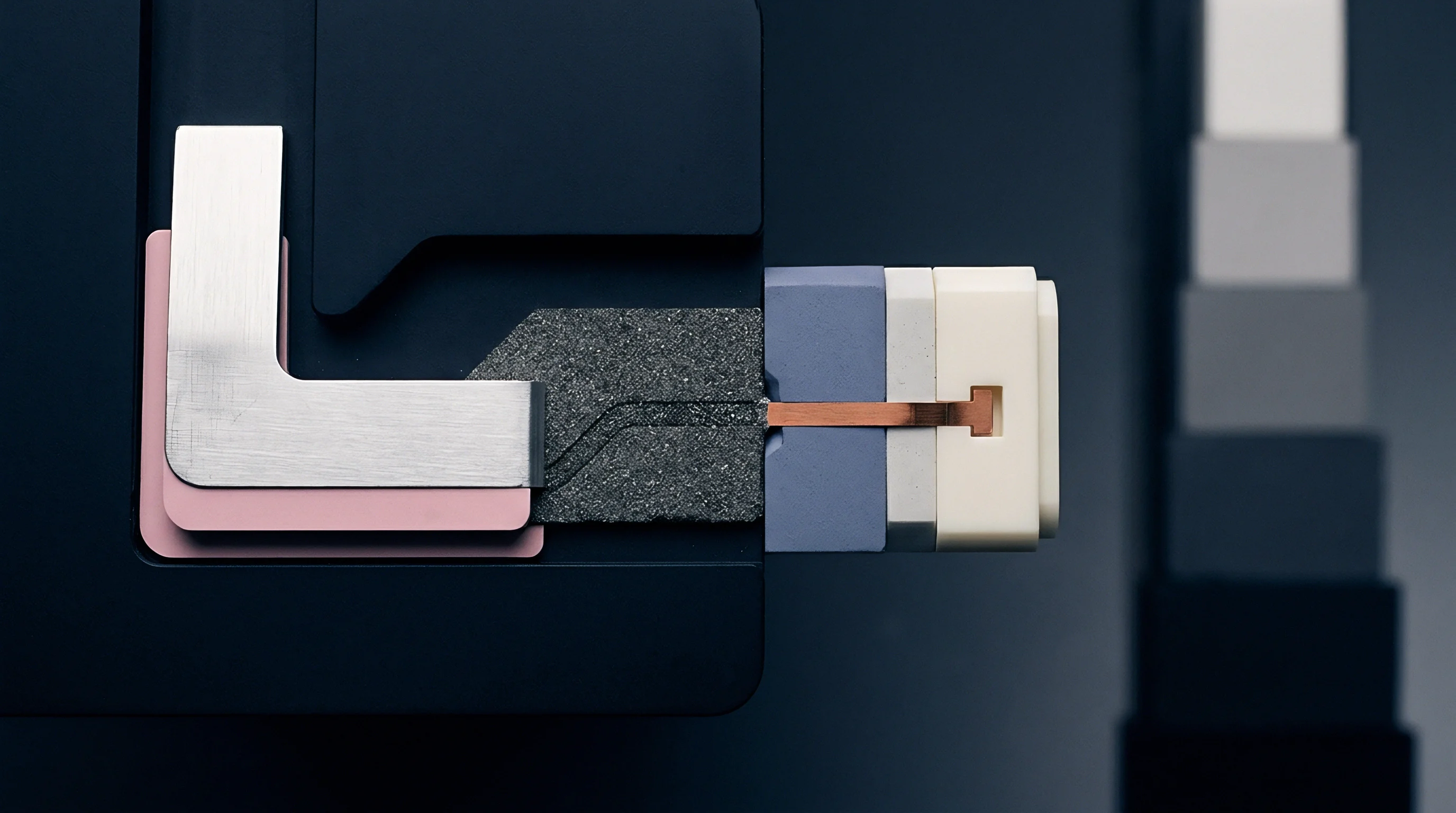
Electrical interconnections crossing from the main circuit board onto a strain-isolated substrate island must traverse narrow bridges. Routing signal, power, and ground traces across these structural ribs demands precise impedance control and stress-relief layout practices to prevent fatigue failure under cyclic mechanical board flexure or thermal vibration. Traces passing across narrow substrate bridges undergo continuous micro-bending, risking copper work hardening and micro-cracking over extended service lifetimes.
High-speed digital interfaces like SPI require controlled characteristic trace impedance, which becomes challenging when crossing narrow substrate bridges with voided ground reference planes beneath the milled slot. Routing differential lines or single-ended traces over an isolated bridge without an adjacent continuous ground return plane generates significant electromagnetic radiation and susceptibility issues. Placing a dedicated ground return trace on an adjacent signal layer within the bridge structure maintains transmission line continuity while ensuring mechanical flexibility remains intact.
Trace Routing across High Compliance Substrate Ribs
Trace width and copper weight selection directly impact the fatigue life of conductors spanning isolation bridges. Standard 1 oz copper (35 µm thickness) rolled-annealed copper offers significantly higher resistance to flexural fatigue failure compared to standard electro-deposited copper. Etching traces into serpentine or curved geometries as they cross the bridge segment redistributes strain along the conductor length, extending fatigue life under cyclic board flexure by more than five times compared to straight, perpendicular trace layouts.
| Interface Type | Max Bridge Width (mm) | Trace Geometry | Ground Return Method | Mean Cycles to Failure |
|---|---|---|---|---|
| Standard I2C (400 kHz) | 1.2 | Straight 0.15 mm | Adjacent Coplanar Trace | 150,000 |
| Precision SPI (10 MHz) | 1.0 | Serpentine 0.12 mm | Embedded Layer 2 Plane | 450,000 |
| Differential Analog | 1.5 | Symmetric Curved Pair | Coplanar Shield Traces | 600,000 |
| Single-Ended Analog | 0.8 | Straight 0.20 mm | No Shielding Plane | 100,000 |
Copper keepouts along the edges of structural support ribs are essential to prevent trace degradation during depanelization operations. Position conductors at least 0.25 mm clear of the rib edge to shield copper from mechanical shear forces during punch or router singulation. Traces running too close to the singulation boundary suffer micro-tears that manifest as intermittent open circuits or elevated conductor resistance under thermal cycling environments.

Which Digital Interface Withstands Substrate Bending Best?
Selecting the digital communication interface for a strain-isolated sensor or voltage reference involves trade-offs between wire count, noise immunity, and physical mechanical compliance across the structural bridge. Serial Peripheral Interface (SPI) protocols require at least four signal lines (SCLK, MOSI, MISO, CS), demanding wider substrate bridges that inherently increase mechanical stiffness and reduce strain isolation efficiency. Inter-Integrated Circuit (I2C) protocols require only two signal lines (SDA, SCL), allowing narrower support ribs that preserve maximum mechanical decoupling of the isolated substrate island.
Internal digital calibration routines are often treated as eliminating the need for mechanical strain isolation. Operational bench testing demonstrates that while onboard digital offset registers compensate for static package stress, dynamic strain caused by board torque and variable thermal gradients continues to induce uncompensated output errors. Reliance on software calibration alone fails to stabilize high-precision measurement circuits subjected to real-world mechanical loading.
Mechanical strain isolation routing provides a necessary physical defense that digital compensation cannot replicate.
- Micro-cracking in Bridge Conductors trace fractures occur along copper grain boundaries due to cyclic mechanical flexure across the isolation gap.
- Capacitance Changes from Edge Distance Shift variable conductor-to-edge clearances alter parasitic trace capacitance, distorting digital bus rise times.
- Cross-Talk Between Paralleled Signal Lines tightly spaced traces running across narrow bridges exhibit high mutual inductance without inter-trace ground shielding.
- Return Current Loop Discontinuity missing reference ground planes under isolation bridges force signal return currents into long, high-inductance loops that elevate radiated EMI.


Yield
Integrating strain isolation slots into printed circuit boards directly impacts manufacturing cost metrics, panel utilization efficiency, and assembly scrap rates. Routing slot channels consumes precious PCB real estate, reducing the overall number of viable boards that fit onto a standard manufacturing panel. Secondary routing operations require extra machine time on expensive CNC milling equipment, adding direct manufacturing costs to every fabricated panel.
Evaluating the financial decision between routing strain isolation slots into a standard laminate substrate versus purchasing pre-isolated ceramic hybrid modules demands thorough make-or-buy break-even analysis. A high-precision bandgap voltage reference in a standard plastic SOIC-8 package mounted on a routed FR4 isolation island costs approximately $3.20 in total component and manufacturing expenses. Purchasing a hermetically sealed, ceramic-packaged voltage reference that naturally resists mechanical stress costs roughly $14.50 per unit.
At production volumes exceeding 10,000 units annually, substrate slot routing yields substantial cost savings despite panel scrap penalties.

Panel Utilization Arithmetic and Secondary Milling Expenses
Standard printed circuit board fabrication relies on high panel density to minimize substrate costs per square inch. Introducing perimeter slot routing requires widening board-to-board spacing within the panel array to accommodate router bit diameters and mechanical debris removal pathways. Standard panel layout clearance increases from 2.0 mm up to 6.0 mm when perimeter strain isolation slots are integrated, reducing total usable panel surface area by 12 percent to 22 percent depending on individual board dimensions.
Assessing a representative manufacturing scenario: a standard 18-inch by 24-inch production panel yields 80 compact sensor PCBs without substrate isolation slots. Integrating C-shaped strain isolation slots increases per-board spacing requirements, dropping panel yield down to 64 boards per panel. Assuming a panel fabrication base cost of $120.00, the raw bare-board unit cost rises from $1.50 up to $1.88 purely due to lost panel utilization.
Laser milling reduces perimeter debris but doubles the thermal heat-affected zone depth along epoxy substrate boundaries.
Secondary CNC milling operations add quantifiable per-panel processing time. Standard board contour routing proceeds at feed rates up to 1.5 meters per minute using a 2.0 mm diameter router bit. Milling intricate strain isolation channels requires smaller 1.0 mm router bits operating at reduced feed rates near 0.6 meters per minute to prevent bit breakage and excess edge burring.
This added milling time increases panel fabrication processing cost by approximately $0.45 per board. Fabrication contracts must incorporate explicit panel utilization factors to prevent unexpected price adjustments when transitioning designs from prototype to high-volume production streams.

Make or Buy Evaluation for Substrate Isolation
Sourcing engineers face clear commercial trade-offs between substrate-level isolation routing, specialized stress-resistant packaging, and standalone signal-conditioned sensor modules. Bare integrated circuit options demand low initial piece-part cost but transfer significant layout, testing, and yield risk onto the internal hardware engineering team. Dedicated pre-packaged modules consolidate mechanical isolation internal to the component body, offering plug-and-play integration at significantly elevated unit purchase prices.
- Mechanical Substrate Routing piece-part cost runs $2.00 to $5.00, engineering bring-up takes 4 weeks, requires moderate PCB surface area, yields 98.2 percent assembly efficiency.
- Hermetic Ceramic IC Packaging piece-part cost runs $12.00 to $25.00, engineering bring-up takes 1 week, requires minimal PCB surface area, yields 99.5 percent assembly efficiency.
- Fully Housed Isolated Sensor Module piece-part cost runs $45.00 to $90.00, engineering bring-up takes 0.5 weeks, requires large external enclosure volume, yields 99.9 percent assembly efficiency.
Selecting the optimal path requires calculating the total landed cost across expected production volumes. For low-volume industrial equipment running below 1,000 units per year, paying the premium for hermetic ceramic packaging or complete standalone modules eliminates engineering development weeks and avoids panel scrap penalties. For high-volume automotive or consumer measurement applications exceeding 50,000 units annually, implementing substrate isolation slot routing on standard FR4 laminates delivers the lowest total cost of ownership across the product life cycle.
Purchasing contracts must incorporate section 4.2 of IPC-6012 to mandate structural integrity verification on all routed substrate isolation features.


Dossier
Fabrication specifications for strain-isolated printed circuit boards require unequivocal dimensional controls, explicit milling tool parameters, and rigorous acceptance sampling protocols. Sourcing documentation must define critical quality characteristics directly on fabrication drawings to ensure PCB vendors deliver compliant substrate assemblies. Vague specifications lead to fabricators altering router bit diameters, feed speeds, or depanelization tab locations without notice, compromising component strain isolation integrity.
Quality audit frameworks for strain-isolated substrates must address dimensional verification of routed channels, edge burr limits, micro-crack inspection, and electrical trace continuity across structural bridge ribs. Automated optical inspection systems programmed specifically to scan isolation channels verify slot widths and keepout boundaries across entire panel arrays. Implementing rigorous incoming quality inspection protocols protects manufacturing lines from assembling expensive high-precision components onto defective substrate lots.

Fabrication Tolerances in Sourcing Technical Specifications
Engineers specifying routed isolation slots must define geometric dimensional tolerances that align with standard fabrication shop capabilities. Specifying overly tight slot width tolerances of ±0.01 mm drives bare-board scrap rates up sharply, as standard CNC routers experience thermal spindle expansion and tool wear that exceed these limits during routine production runs. A realistic, achievable slot routing tolerance specification stands at ±0.05 mm, which provides sufficient mechanical consistency without incurring precision machining cost penalties.
Copper keepout definitions require unambiguous dimensional callouts on Gerber manufacturing layers. Drawings must state that all internal and external copper layers maintain a minimum 0.35 mm clearance from the finished, milled slot edge, inclusive of router bit positional tolerance. Explicitly specifying that no copper plating shall exist on internal slot walls prevents short circuits caused by conductive copper dust dragging across inner layers during milling.

Quality Sign-off Criteria for High Precision PCB Substrates
Establishing clear sign-off criteria for bare PCB substrate lots incoming from fabrication vendors prevents non-compliant boards from reaching SMT assembly lines. Cross-sectional micro-sectioning of sample boards from each panel production lot verifies that perimeter milling operations did not cause internal layer delamination or micro-fracturing extending into signal routing channels. Acceptance criteria mandate zero micro-delamination extending more than 0.05 mm beyond the milled edge boundary.
Lot acceptance protocols require optical coordinate measurement verification of isolation tab widths and mouse bite hole diameters. Rib widths measuring outside the specified ±0.08 mm tolerance band are rejected, as undersized tabs risk prematurely fracturing during component placement while oversized tabs exert excessive mechanical stress on components during final depanelization. Electrical continuity and isolation resistance testing across support bridges ensures zero trace damage or high-impedance leakage paths before surface-mount component population proceeds.
Hardware sourcing practices that incorporate these technical validation criteria achieve predictable, repeatable strain isolation performance across global manufacturing supply chains.