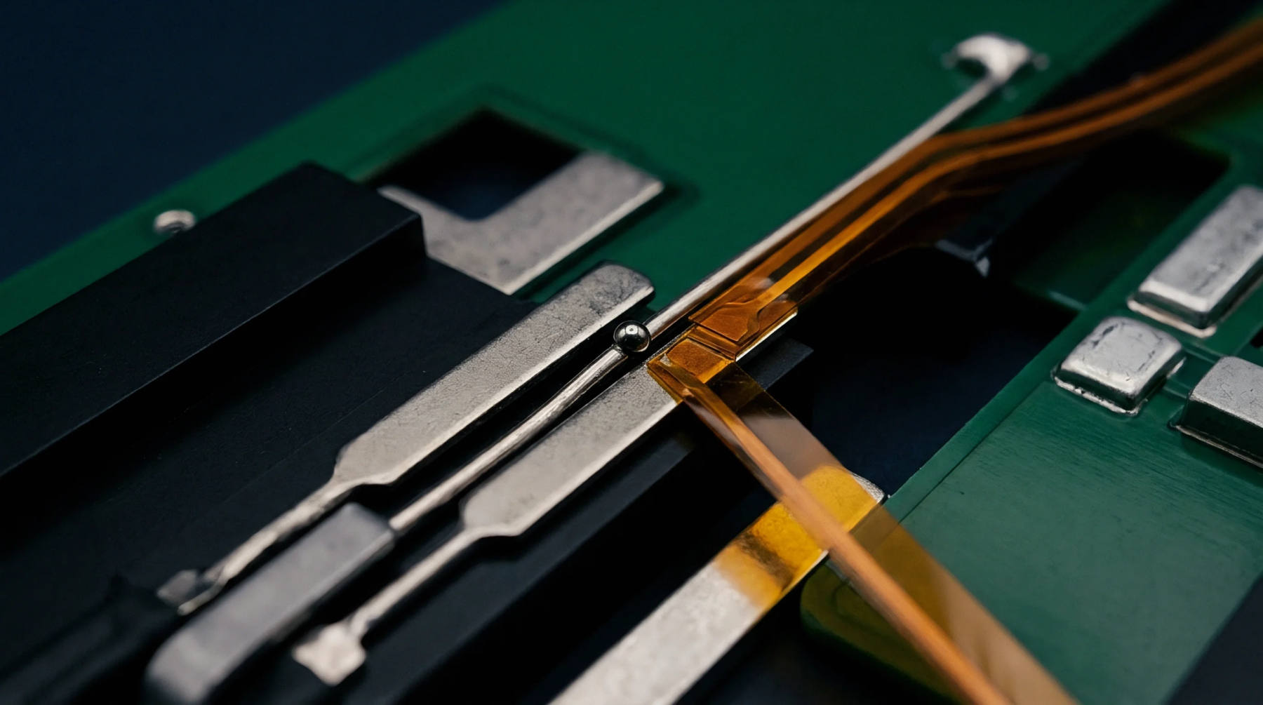
Single Point Topology
Centralized reference nodes connect multiple circuit returns at a single physical point to eliminate common impedance coupling between distinct subsystem currents. In precision sensor instrumentation and high-resolution data acquisition boards, star grounding isolates sensitive analog signal returns from high-current digital return paths. Separate copper traces run from each ground zone to the central reference stud or dedicated plane connection.
Improper topology allows heavy ground currents to modulate the reference potential of microvolt-level analog signals.
Ground Loop Mitigation
Loop currents driven by stray magnetic fields create differential error voltages across distributed ground connections. Connecting chassis earth and signal ground at only one central point breaks conductive loops that introduce mains ripple into sensitive measurement channels. High-frequency RF circuits require low-impedance ground planes rather than single point connections due to trace inductance.
Substrate Coupling
Parasitic inductance in long ground leads causes high-frequency return currents to find alternative capacitive paths through board substrate materials. Trace geometry and conductor width control the self-inductance of individual ground branches in star grounding layouts. High peak current pulses from switching regulators generate voltage spikes across long return traces, corrupting nearby analog reference nodes.
Printed circuit board designers keep return path lengths short while maintaining isolated physical paths back to the main power return point. Instrument qualification verifies ground isolation resistance using mega-ohmmeter testing prior to power application.
Return Path Verification
Automated continuity and impedance testing validates isolation between analog and digital ground domains prior to power component installation. Vector network analyzers measure ground transfer impedance across frequency sweeps from ten hertz to ten megahertz to identify unintended resonant loops. Noise floor measurements on high-bit ADC evaluation boards confirm that switching noise remains below specified microvolt thresholds under full digital processing loads.
Documentation certifies ground node potential differences stay within millivolt tolerances across all operating modes.