Diagnosing Low-Level Electrical Faults on I2C Buses
Systematic I2C electrical fault diagnosis requires measuring line capacitance, verifying logic voltage margins, and analyzing bus edge transition dynamics.
Trace
Interconnect physical properties govern the charge and discharge timing of open-drain signal lines. Because an I2C bus uses passive pull-up resistors to pull serial clock (SCL) and serial data (SDA) lines high while active open-drain transistors pull them low, edges behave asymmetrically: rising transitions follow an RC charging curve, while falling transitions snap down through current sinking. Faults appear when parasitic capacitance from board traces, package pins, or external wiring exceeds driver sink limits or drags rise times past standard logic threshold windows.
Capacitance and Pull-Up Calculations
Sizing pull-up resistors requires balancing maximum allowable signal rise time against the sink capacity of the bus drivers. Standard mode at 100 kHz permits a maximum rise time (tr) of 1000 nanoseconds, whereas fast mode at 400 kHz tightens tr to 300 nanoseconds. Total bus capacitance (Cb) accumulates across trace runs, pin input capacitance at every connected device, and stray wiring coupling, with each additional picofarad dragging out the RC time constant.
The upper resistance limit (Rpullup(max)) keeps the RC rise time within specification according to:
Rpullup(max) = fractr0.8473 × Cb
At the other end, minimum resistance (Rpullup(min)) prevents driver saturation, ensuring the line pulls down to an output low voltage (VOL) below 0.4 V at a nominal sink current (IOL) of 3 mA:
Rpullup(min) = fracVDD – VOL(max)IOL
On a 3.3 V rail with standard 3 mA sink drivers, this sets the absolute lower resistance limit at 967 ohms. Pulling up with too much resistance rounds off signal peaks before they can cross receiver input thresholds.
Maximum bus capacitance of 400 pF limits standard mode operation to pull-up resistance values above 1.08 kilohms.
Physical Channel Loading in Compact Substrates
Die pin footprints and board dielectric constant determine the baseline lumped capacitance of each signal line. Surface-mount packages introduce variable parasitic capacitance per pin: WLCSP adds 0.5 pF to 1.2 pF, QFN packages contribute 1.5 pF to 2.5 pF, while leaded SOIC packages add up to 4.0 pF per pin. Trace routing on standard FR-4 substrates (dielectric constant εr = 4.3) adds approximately 1.5 pF to 2.0 pF per inch for 5-mil trace widths over a solid ground plane.
Interconnect cables extending off-board contribute 15 pF to 30 pF per foot, quickly exhausting the 400 pF specification limit established in UM10204.
| Operating Mode | Max Clock Frequency | Max Bus Capacitance (Cb) | Max Rise Time (tr) | Max Fall Time (tf) | Min Pull-Up (Rpullup) at 3.3V |
|---|---|---|---|---|---|
| Standard Mode (SM) | 100 kHz | 400 pF | 1000 ns | 300 ns | 967 Ω |
| Fast Mode (Fm) | 400 kHz | 400 pF | 300 ns | 300 ns | 967 Ω |
| Fast Mode Plus (Fm+) | 1000 kHz | 550 pF | 120 ns | 120 ns | 145 Ω (IOL=20 mA) |
| High Speed Mode (Hs) | 3400 kHz | 100 pF | 40 ns | 10 ns | Active Current Source |
If pull-ups are oversized on heavily loaded traces, the line fails to reach 70 percent of supply voltage before the clock period closes. That leaves the bus vulnerable to intermittent acknowledgment misses, dropped bytes, and lockups that come and go with temperature swings.

Waveform
Signal integrity breaks down quickly when parasitic inductance and bus contention distort edge transitions. Isolating these faults requires high temporal resolution to catch ringing, undershoot, and illegal intermediate logic states, separating raw channel physics from driver-level protocol conflicts.
Deconstructing Bus Contention and Stuck Lines
When a target device misses a clock pulse, it often holds SDA low waiting for remaining bits, which the host interprets as a constant low state, stalling the entire channel. Contention also develops if two masters arbitrate simultaneously, or if a target asserts data during a high clock phase without supporting clock stretching.
Engineers evaluate physical bus anomalies against specific waveform criteria:
- Stuck Data Low State reflects a target state machine lockup where SDA remains continuously below 0.4 V despite host SCL toggling.
- Bus Contention Plateau appears as an intermediate voltage level (typically between 0.8 V and 1.8 V) caused by competing drivers or resistive shorts.
- Slow Edge Relaxation manifests as an exponential charging curve exceeding maximum rise time limits, preventing receiver input threshold crossing.
- Inductive Ringing Spikes present high-frequency AC oscillations crossing receiver switching thresholds after fast falling edges.
When steep falling edges drive sharp current steps through long trace stubs, trace inductance and ground bounce produce voltage undershoot below -0.5 V relative to ground, setting off inductive ringing that trips false clock edges.
UM10204 section 6.1 specifies maximum allowable signal rise time as 1000 nanoseconds for standard mode and 300 nanoseconds for fast mode.
Transient Suppression and Edge Dynamics
Reflections from fast clock edges can step through receiver threshold regions prematurely. Installing small damping resistors (Rs = 10 Ω to 33 Ω) directly at driver pins absorbs these inductive reflections without dragging out rise times, giving downstream targets clean transitions free of multiple-clocking glitches.
| Observed Waveform Symptom | Physical Root Cause | Electrical Parameter Deviation | Corrective Action |
|---|---|---|---|
| Mid-rail voltage step during ACK | Contention between host and target drivers | Current draw spikes; VSDA sits between VIL and VIH | Adjust bit timing; verify target address assignment |
| Exponential rise curve exceeding tr limit | Excessive line capacitance or high Rpullup | RC time constant > 300 ns in Fast Mode | Reduce Rpullup value; shorten trace length |
| Negative spike below -0.5V on falling edge | Unterminated stub inductance and fast fall time | L · (di/dt) overshoot exceeding ESD diode threshold | Add 10 Ω to 33 Ω series damping resistor at driver |
| Constant 0.2V floor on SDA | Target IC locked in active output state | Target driver low-side N-channel FET continuously active | Issue 9 clock pulses on SCL; execute hardware reset |
Bus lockups are routinely blamed on firmware timing rather than silicon behavior, though hardware traces confirm that target state machines freeze when glitch spikes land on clock inputs during active transmission windows.


Ground
Common-mode ground shifts between nodes distort logic-low thresholds across longer runs. When sensors sit on separate boards or remote sub-assemblies, return currents from nearby power stages elevate the target’s ground reference relative to the host, altering the net voltage seen at the receiver pins.
Common-Mode Shift and Crosstalk Coupling
Return current paths shared with high-current switching loads elevate local target potential relative to host receiver inputs. An offset voltage (VGND(offset)) shifts perceived low voltage from VOL to VOL + VGND(offset). When total voltage exceeds the maximum low-level input threshold (VIL(max) = 0.3 × VDD), target receivers interpret a low state as high, causing immediate packet corruption.
Parallel runs in flat ribbon cables encourage capacitive cross-coupling between clock and data lines. Fast dV/dt edges on SCL induce transients on adjacent SDA conductors; once these spikes exceed receiver hysteresis limits, they generate phantom START or STOP conditions that derail transactions.
Common-mode ground offsets between isolated targets compress receiver noise margins and cause false start bit detection.
Cable Routing and Shielding Guidelines
Adjacent placement of serial clock and serial data conductors in ribbon wiring induces mutual capacitive spikes during state transitions. Interleaving signal wires with ground lines suppresses electric field coupling between clock and data channels. Standard conductor mapping assigns ground lines between active signal conductors: GND, SDA, GND, SCL, GND, VDD.
This arrangement shields data signals from clock edge transients while maintaining uniform line impedance.
Galvanic isolation techniques isolate high-noise targets operating across elevated ground potentials. Optocouplers or digital capacitive isolators separate electrical domains while transmitting open-drain logic states. Optocoupler isolators require bi-directional current buffers to manage open-drain directionality without latching lines in a low state.
Layout verification must ensure ground plane splits never cross beneath open-drain signal traces, where return path discontinuities form slot antennas that radiate wideband electromagnetic interference.

Margin
Voltage threshold windows shrink when multi-rail translation components and thermal coefficient shifts alter standard logic levels. Modern mixed-voltage systems operate nodes at 1.8 V, 2.5 V, 3.3 V, and 5.0 V supply levels on a unified bus network. Bi-directional level translators bridge these voltage domains, but introduce parasitic pass-gate series resistance, leakage current offsets, and supply rail tracking errors.

When Does Input Threshold Drift Cause Bus Lockup?
Rising die temperatures increase pin leakage while lowering driver transistor saturation conductance. Leakage currents (ILI) drawn through high-value pull-up resistors pull VOL upward and drag VOH downward. Because standard CMOS thresholds track supply rails ~ VIL(max) = 0.3 × VDD and VIH(min) = 0.7 × VDD ~ operating at high temperatures erodes noise margins until valid transitions land in undefined logic territory.
| Supply Voltage (VDD) | Max Input Low (VIL(max)) | Min Input High (VIH(min)) | Max Output Low (VOL(max)) | Min Noise Margin Low (NML) |
|---|---|---|---|---|
| 1.8 V | 0.54 V | 1.26 V | 0.36 V | 0.18 V |
| 2.5 V | 0.75 V | 1.75 V | 0.40 V | 0.35 V |
| 3.3 V | 0.99 V | 2.31 V | 0.40 V | 0.59 V |
| 5.0 V | 1.50 V | 3.50 V | 0.40 V | 1.10 V |
Pass-gate level translators rely on N-channel MOSFETs biased by a reference gate voltage. When bridging 1.8 V and 3.3 V rails, the pass-gate switch adds channel resistance (RON ≈ 10 Ω to 30 Ω) directly in series with the low-side driver’s saturation resistance, elevating the logic low voltage measured at the target pin.
Series damping resistors positioned near driver output pins suppress high-frequency ringing without degrading signal rise times.
Bi-Directional Level Translation Dynamics
Passive level shifting adds series resistance that slows fall times and raises low-state offsets. Active bi-directional translators attempt to counter this by firing internal edge-rate accelerators: when they detect a rising edge, high-current P-channel FETs turn on for tens of nanoseconds to charge bus capacitance rapidly.
Conflict arises when edge accelerators fire during slow, valid logic transitions or during clock stretching routines. Spurious current injection from edge accelerators distorts clock line low phases, corrupting transaction timing. Selecting level translators requires matching accelerator response times to expected bus capacitance limits.
Designing bus channels with elevated pull-up values without accounting for high-temperature pin leakage guarantees intermittent field failures.

Diagnostics
Isolating faults requires disciplined probing and physical channel segmentation. Standard 10x passive probes present 10 pF to 15 pF of capacitance per channel, which is often enough to alter rise times and mask the very capacitance issues under investigation.
Bench Oscilloscope Probing and Signal Capture
Standard passive 10:1 probes add baseline capacitive loading during physical pin measurements, whereas high-impedance active FET probes (Cin) minimize channel disturbance.
To systematically isolate electrical failures on complex bus segments, engineers execute a disciplined measurement workflow:
- Connect active FET probes to host controller SDA and SCL pins using short ground springs.
- Capture baseline rise times (tr) and fall times (tf) under nominal operating loads.
- Measure low-level output voltage (VOL) during target ACK bit transmission phases.
- Apply local heating to target ICs to evaluate thermal leakage drift on VOL levels.
- Verify that logic high levels achieve at least 70 percent of local VDD supply voltages.
Logical Isolation Protocol
Sequential disconnect of peripheral target boards narrows fault locations to specific bus branches. Bus switch multiplexers (such as PCA9548A) isolate downstream capacitive channels while resolving I2C address collision conflicts. Isolating broken bus segments prevents localized short circuits from disabling primary host control channels.
Standard IPC-A-610 criteria require solder joints on bottom-terminated surface-mount packages to exhibit complete wetting without micro-bridging beneath low-gap packages. Solder bridging between adjacent pins on 0.5 mm pitch DFN components creates resistive shorts that hold lines at intermediate logic voltages.
Package
Selecting component package forms dictates land pattern geometries, thermal dissipation properties, and line parasitic capacitance. Mechanical stress induced during board reflow alters internal die characteristics, shifting sensor calibration and pin leakage parameters. Choosing package formats requires evaluating electrical performance alongside manufacturing assembly yield and landed component cost.
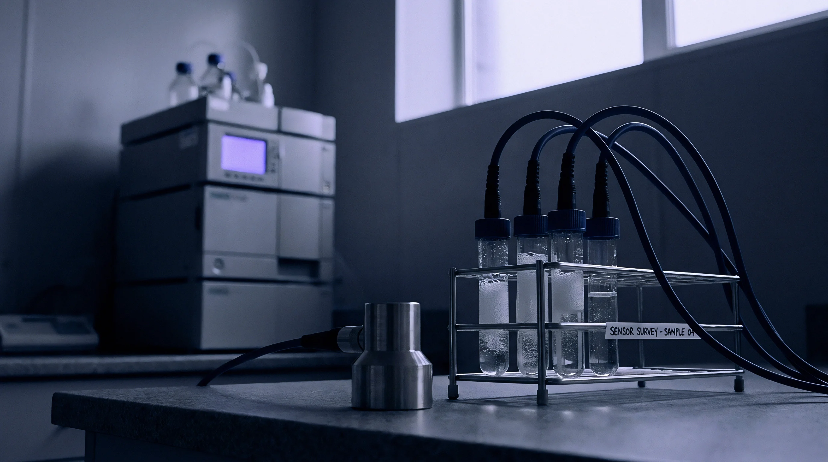
Sourcing Trade-Offs and Land Pattern Physics
Bare die integration using Wafer Level Chip Scale Packaging (WLCSP) minimizes footprint and parasitic pin capacitance.
Integrating sensors into harsh industrial environments often forces a transition from board-level SMD packages to cabled standalone assemblies. Standalone housed modules incorporate internal level translation, transient voltage suppression (TVS) diodes, and bus buffering ICs. TVS diodes protect sensitive inputs from electrostatic discharge but contribute significant parasitic capacitance ($15 pF to 100 pF per diode), drastically reducing maximum usable wire run lengths.
Component selection balances initial unit purchase price against software driver development costs, stencil aperture design effort, and incoming quality verification testing. Small package formats lower unit cost and conserve board real estate, but demand tight land pattern process controls to prevent assembly defects that manifest as low-level electrical bus faults.