Cryogenic Strain Decoupling Architectures for Wafer Level Packaging
Cryogenic strain decoupling architectures protect wafer-level readout packages by replacing rigid solder joints with compliant Indium or spring interconnects.

Shrink
Cooling from room temperature down to four Kelvin subjects mixed packaging materials to extreme shear. Monocrystalline silicon has a non-linear expansion coefficient that drops from 2.6 parts per million per Kelvin at 293 Kelvin to near zero below 20 Kelvin, briefly dipping into negative values around 120 Kelvin. Organic substrates, ceramic carriers, and printed circuit boards shrink much faster, ranging from 6 parts per million per Kelvin for alumina up to more than 15 parts per million per Kelvin for FR4 laminates.
When a wafer-level packaged readout chip mounts directly to a carrier board, the resulting mismatch creates lateral displacement gradients across the bump array.
Without an isolation architecture, this strain passes straight into the active silicon device layer. In cryogenic sensor applications such as infrared focal plane readout integrated circuits, superconducting quantum interference device amplifiers, and cryogenic CMOS sensor interfaces, mechanical stress shifts the piezoresistive coefficients. That alters carrier mobility in transistor channels, moving gate threshold voltages by up to thirty millivolts and undermining bias stability across low-noise front ends.
Left unmitigated, strain alters sensor offsets and introduces drift profiles that calibration cycles cannot eradicate.
Differential contraction between monocrystalline silicon and alumina substrates reaches 2.8 micrometers per millimeter when cooled from 293 Kelvin down to 77 Kelvin.
Calculating the thermal displacement vector requires integrating the differential thermal expansion coefficient across the full operational temperature drop. Cumulative strain scales with distance from the neutral point of the die assembly, concentrating maximum shear force at the outer corner interconnects of large-format chips.

Carrier Mobility Shifts under Cryogenic Stress
Stress distorts the crystal lattice symmetry in silicon, altering its energy band structure. In p-channel metal-oxide-semiconductor transistors, compressive stress splits the heavy-hole and light-hole valence bands, modifying hole effective mass and boosting transconductance. In n-channel devices, triaxial stress alters the conduction band valley degeneracy instead, raising electron scattering and lowering mobility below 77 Kelvin.
When packaging strain varies spatially across a wafer-level die, neighboring transistors within differential pair circuits experience unequal stress states, generating offset errors in high-resolution signal chains.
At cryogenic temperatures, lattice stiffness increases, reducing the plastic yield capability of silicon and metallic interconnects. Stresses that cause minor viscoelastic relaxation at room temperature cause brittle fracture or permanent piezoelectric zero-point offsets in cryogenic sensors. Strain decoupling architectures isolate the sensitive die from structural substrate movements, preserving designed signal conversion performance.
| Material | Mean CTE 300K-77K (10^-6/K) | Mean CTE 77K-4K (10^-6/K) | Young Modulus 300K (GPa) | Young Modulus 4K (GPa) |
|---|---|---|---|---|
| Monocrystalline Silicon (100) | 1.35 | 0.05 | 130 | 135 |
| Borosilicate Glass (Pyrex 7740) | 2.10 | 0.25 | 64 | 68 |
| Alumina Ceramic (99.5% Al2O3) | 4.80 | 0.30 | 370 | 390 |
| High-Purity Indium (In) | 25.10 | 12.40 | 11 | 14 |
| Polyimide Film (PI) | 32.00 | 8.50 | 3.1 | 5.8 |
| Copper (OFHC) | 13.20 | 1.80 | 117 | 138 |
The point where piezoresistive shift transitions from an offset error into permanent crystal lattice dislocation remains debated across cryogenic foundry characterization programs.
Flex
Compliant structures intercept strain propagation between the system board and the wafer-level package. Adding elastic or micro-spring interfaces allows differential thermal contraction to express as localized structural deflection rather than die-level stress. Micro-machined silicon springs, high-aspect-ratio Indium pillars, and polymer redistribution layers serve as the primary structural mechanisms deployed in cryogenic packaging.
Indium maintains high ductility at cryogenic temperatures. Unlike lead-tin or lead-free solders that turn brittle below 150 Kelvin, pure Indium retains plastic deformation capability down to liquid helium regimes. High-aspect-ratio Indium micro-pillars, fabricated via electroplating or thermal evaporation through deep photoresist masks, absorb lateral shear through bending deformation.
Increasing the pillar aspect ratio reduces the transverse spring constant, effectively isolating the wafer die from thermal movement.
Compliant interconnect height ought to match or exceed the maximum anticipated lateral thermal displacement.
Air-gap through-silicon via strain relief architectures surround vertical interconnects with micro-machined annular voids. These voids isolate the conductive copper core from the bulk silicon substrate, preventing differential radial thermal expansion of the copper from cracking the surrounding die matrix during repeated thermal cycling.

Structural Strategies for Strain Mitigation
Polymer redistribution layers provide localized compliance beneath bond pads. Viscoelastic polymers such as photosensitive polyimide and benzocyclobutene act as mechanical buffers between metallic redistribution tracks and brittle low-dielectric-constant silicon oxide layers.
- Interconnect Solder Joint Shear Fatigue occurs when rigid interconnect arrays are pushed beyond their elastic limit during thermal cycling, leading to crack initiation at the pad interface.
- Low-k Dielectric Delamination develops when high thermal mismatch stresses transmit into brittle sub-micron oxide layers located directly below bump pads, causing functional signal loss.
- Silicon Substrate Microcracking results from concentrated stress points at the edges of rigid through-silicon vias during rapid cooldown cycles.
- Piezoresistive Transistor Threshold Drift occurs when residual strain fields propagate into active channel regions, shifting analog bias points and gain coefficients.
Compliant interconnects prevent substrate shear fracture. Implementing cantilever micro-springs on the wafer surface allows high-density area-array bonding while maintaining lateral compliance exceeding 0.5 micrometers per millinewton.
| Architecture Type | Aspect Ratio Range | Lateral Compliance (mm/N) | Electrical Resistance (mOhm) | Pitch Limit (um) |
|---|---|---|---|---|
| High-Aspect Indium Pillars | 3:1 to 5:1 | 0.12 – 0.28 | 12 – 25 | 20 |
| Cantilever MEMS Springs | 4:1 to 8:1 | 0.45 – 0.95 | 45 – 110 | 50 |
| Polyimide Buffer Layer RDL | 1:2 to 1:1 | 0.05 – 0.10 | 5 – 12 | 15 |
| Annular Air-Gap TSV | 8:1 to 15:1 | 0.18 – 0.35 | 8 – 18 | 35 |
| Data measured across test vehicles subjected to 300 K to 77 K immersion cycles; compliance calculated at maximum lateral deflection limit. | ||||
Designing compliant interconnect structures requires balancing lateral flexibility against high-frequency signal integrity, as longer spring paths increase parasitic lead inductance.
Frost
Cryogenic operational environments expose packaged integrated circuits to extreme thermal shock and extended low-temperature exposure. Thermal cycling between 293 Kelvin and 77 Kelvin in liquid nitrogen, or down to 4.2 Kelvin in liquid helium dewars, induces transient thermal gradients across the wafer-level package. When one edge of a chip cools faster than the core, dynamic temperature gradients generate transient stress fields that exceed steady-state cryogenic strain values.
Polymer underfills harden below their glass point. Standard epoxy capillary underfills designed for room-temperature board assembly become exceptionally brittle below 150 Kelvin. The coefficient of thermal expansion of conventional underfills drops precipitously, but their Young’s modulus increases up to three-fold.
A hardened underfill locks the bump array into a rigid composite block, transferring substrate displacement directly into the silicon die and causing catastrophic delamination of the active circuit layer.
Polymer underfill materials transitioning below their glass point transform lateral compliance into rigid mechanical transfer.
Underfill-free packaging designs utilize open air-gap architectures or localized silicone-based compliant buffers that maintain elastomeric properties at low temperatures. Eliminating rigid underfill material preserves the freedom of Indium micro-pillars or MEMS springs to flex laterally during thermal transition cycles.

Where Does Indium Fatigue Surface during Cryogenic Cycling?
Repeated thermal shock testing forces Indium interconnects through cyclic plastic deformation. Although Indium remains ductile at liquid helium temperatures, thermal cycling causes grain boundary sliding and recrystallization within the micro-bumps. Over hundreds of cycles between 300 Kelvin and 77 Kelvin, micro-voids coalesce along grain boundaries, generating shear fatigue cracks that propagate across the narrowest cross-section of the bump.
- Mount the wafer-level package into a liquid nitrogen bath immersion chamber operating with dry nitrogen purging to prevent moisture condensation.
- Cool the assembly at a controlled ramp rate not exceeding ten Kelvin per minute down to 77 Kelvin, monitoring four-wire electrical resistance across daisy-chained bump paths continuously.
- Dwell at 77 Kelvin for twenty minutes to achieve complete thermal equilibrium across heterogeneous material interfaces.
- Heat the assembly back to 293 Kelvin using infrared radiative heating elements at a rate of fifteen Kelvin per minute.
- Record high-resolution resistance logs to identify micro-fracture initiation points marked by localized resistance spikes.
Microcracks degrade electrical path continuity under cold. Failure to decouple thermal strain leads to open-circuit faults, catastrophic substrate cracking, and total loss of sensor readout functionality during operational missions.
Inspection
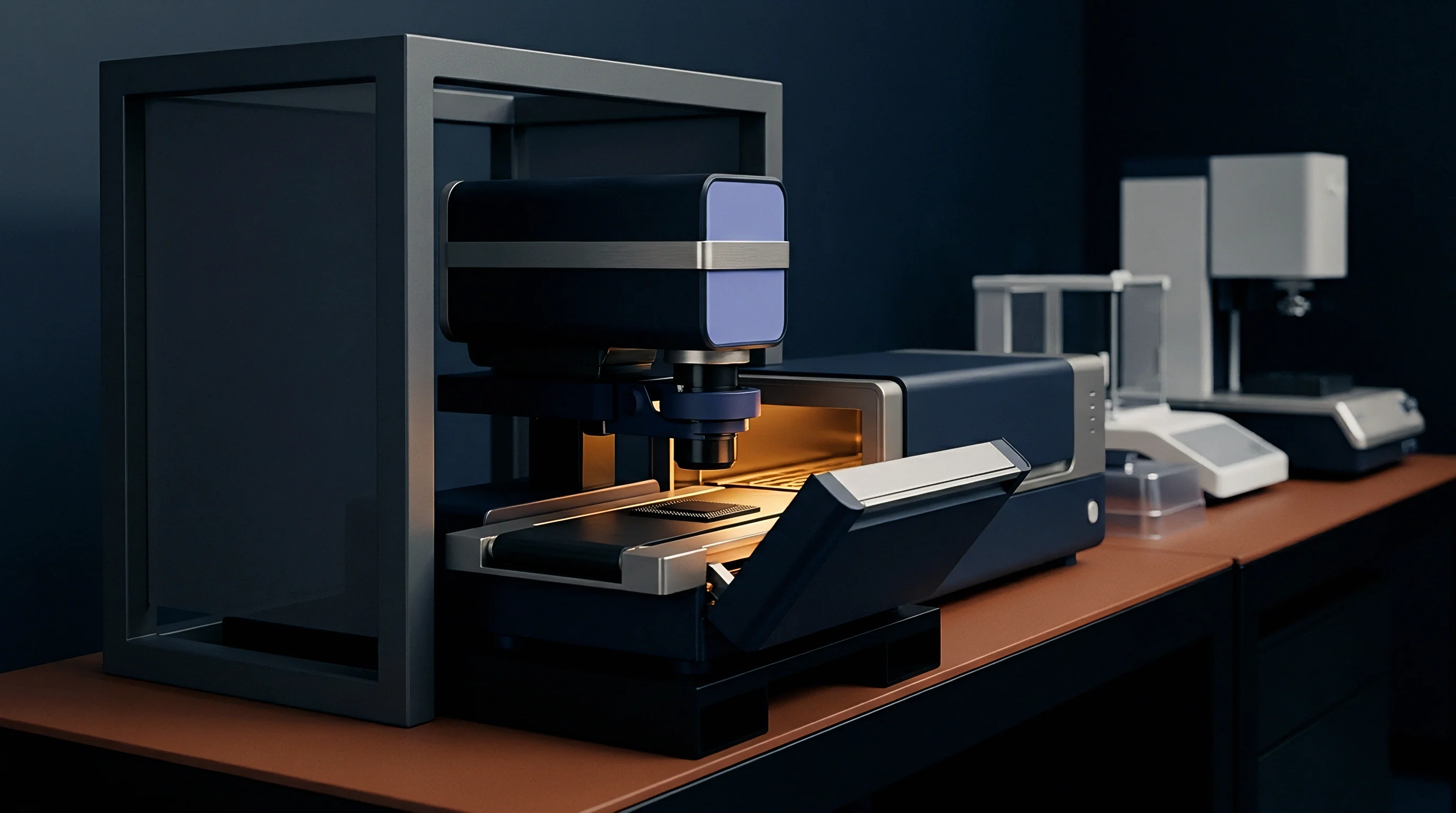
Nondestructive diagnostic methods verify structural integrity within cryogenic packages before and after thermal stress testing. Conventional optical inspection cannot evaluate buried bump arrays or internal through-silicon via interfaces. High-resolution scanning acoustic microscopy, X-ray micro-tomography, and cryogenic laser interferometry provide the primary physical metrics required to audit strain decoupling performance.
Scanning acoustic microscopy utilizes high-frequency ultrasound transducers ranging from 100 MHz to 230 MHz to detect sub-micron delamination gaps between the silicon die, redistribution layers, and interconnect bumps. Sound waves reflect strongly off air interfaces caused by delamination or microcracks, yielding high-contrast acoustic images of hidden structural failures within the package stack.
Compliance with MIL-STD-883 Method 1010 Condition D demands fifty temperature shocks without joint detachment.
Laser interferometry tracks dynamic out-of-plane displacement across the die surface during thermal cooling. Profiling warpage maps in real-time allows signal-chain engineers to locate localized stress concentrations and validate mechanical finite-element models against observed bench performance.
Diagnostic Toolsets for Cryogenic Package Audits
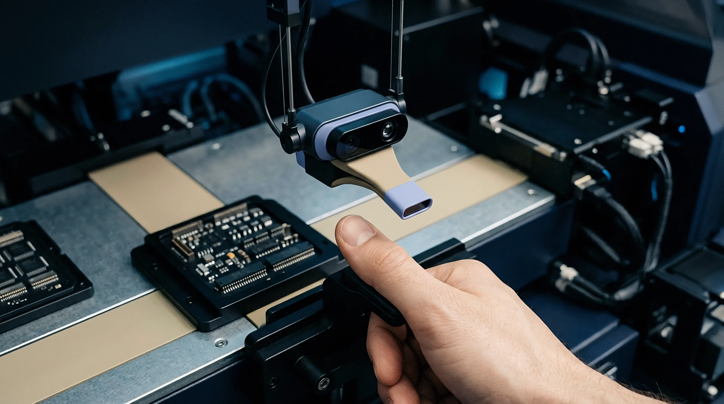
Electrical resistance mapping using four-wire Kelvin structure arrays provides quantitative real-time monitoring of bump strain state during cryogenic exposure. Small increases in path resistance signal the onset of necking or micro-void formation within Indium pillars before complete open-circuit failure occurs.
| Diagnostic Technique | Physical Signal Measured | Spatial Resolution | Cryogenic In-Situ Capable |
|---|---|---|---|
| C-Mode Scanning Acoustic Microscopy | Acoustic impedance boundaries | 5 micrometers | No (Room Temp Only) |
| X-Ray Micro-Computed Tomography | X-ray attenuation density | 1 micrometer | Yes (With Cryo-Stage) |
| Digital Holographic Interferometry | Optical phase shift | 10 nanometers (Z-axis) | Yes (Windowed Cryostat) |
| Four-Wire Kelvin Probe Array | Voltage drop at fixed current | Single bump node | Yes (Continuous Logging) |
Verification requires proving structural stability under maximum operational thermal cycling loads.
- Acoustic Delamination Threshold defines the maximum allowable cumulative area of interface voiding detected via acoustic microscopy before lot rejection occurs.
- Maximum Dynamic Warpage Limit sets the peak out-of-plane distortion permitted across the active pixel matrix during transient cooling cycles.
- Kelvin Resistance Stability Criterion specifies that individual bump resistance shifts must remain below five percent over one hundred deep thermal cycles.
- Hermeticity Retention Level verifies that seal ring structures maintain helium leak rates below 10^-8 atmosphere cubic centimeters per second after cryo-shock.
Bump array delamination can stem from unoptimized customer reflow profiles or inherent thermomechanical stress concentrations within rigid underfill layers.

Allocation
Procuring wafer-level packages engineered for cryogenic operations requires establishing clear manufacturing specifications and vendor qualification criteria. Standard commercial wafer-level packaging processes target industrial temperature ranges from minus forty to one hundred twenty-five degrees Celsius. Adapting these production lines for cryogenic service demands specialized material sets, modified non-recurring engineering tooling, and stringent incoming inspection protocols.
Dual foundry sourcing mitigates mask tooling delays. Custom mask sets for Indium pillar electroplating and high-aspect-ratio redistribution layers involve substantial capital commitment, making second-source qualification an operational necessity for high-reliability aerospace and scientific instrumentation programs.
Cryogenic packaging demands specialized cleanroom assembly tooling. Sourcing partners must demonstrate cleanroom environment controls capable of handling soft metallic interconnects like Indium without surface oxidation or particle contamination that compromises cold weld joint formation.
Commercial Verification and Dossier Requirements
Contractual procurement specifications for cryogenic wafer-level packages must mandate full traceability from raw material ingots to final packaging assembly. Indium purity levels must meet 99.999 percent requirements to prevent localized phase transformations or intermetallic embrittlement at low temperatures.
- Raw Material Certificate of Conformance documenting chemical purity and gas analysis for all deposition targets and plating chemistries.
- Cryogenic Thermal Cycling Test Report detailing four-wire electrical tracking logs across representative test vehicles over a minimum of fifty cycles down to 77 Kelvin.
- Acoustic Microscopy Scan Dossier providing baseline and post-cycling C-SAM imagery for one hundred percent of delivered flight-grade or high-reliability lots.
- Failure Analysis Protocol Master Document defining destructive physical analysis procedures for lot acceptance sampling.
Sole sourcing exposes projects to foundry disruption. Contracts must explicitly define ownership of custom packaging process design rights and non-recurring engineering tooling assets to allow seamless transfer between alternate packaging foundries when primary supply chains fail.
Standard delivery contracts must incorporate MIL-STD-883 Method 1010 Condition D testing clauses, enforcing supplier financial liability for lot rejections stemming from verified interconnect delamination during cryogenic qualification screening.