Protective Enclosure
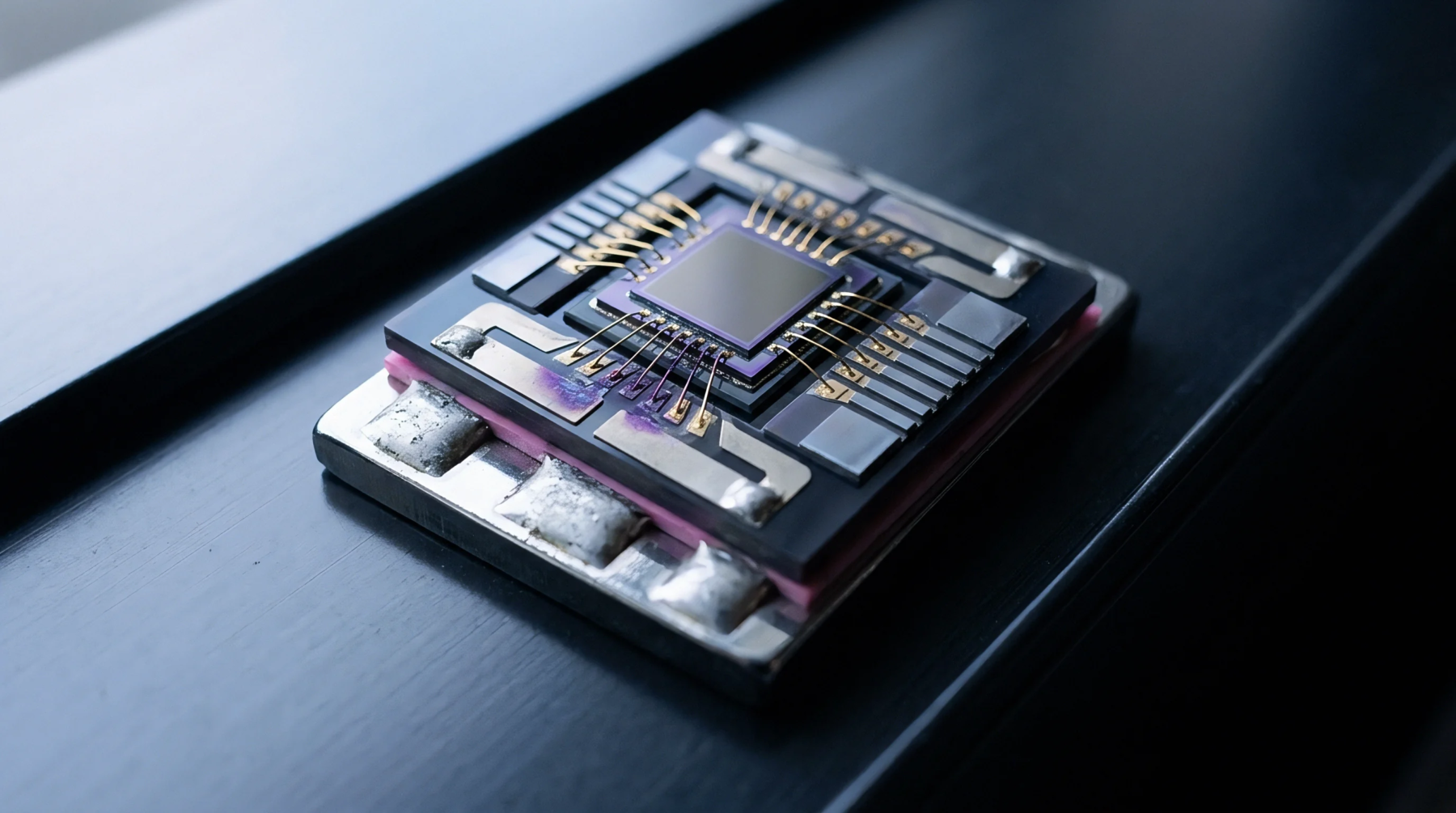
Specialized semiconductor housings isolate micro-electromechanical structures from ambient environmental contamination while maintaining mechanical stress boundaries. MEMS sensor packaging seals delicate silicon structures inside hermetic or gel-filled cavities. The package provides electrical interconnects via bond wires or TSVs while shielding internal components from moisture and corrosive gases.
Structural design governs how mechanical forces transfer from circuit boards to sensitive internal elements.
Mechanical Coupling
Packaging materials with mismatched coefficients of thermal expansion generate mechanical stress across temperature cycles. Thermal strain transfers into silicon sensor dies, inducing offset voltage drift and sensitivity alterations. Cavity design and die attach selection decouple external package deformation from suspended micro-structures.
Gel fill materials protect exposed surfaces but transfer hydrostatic pressure changes to mechanical elements.
Thermal Hysteresis
Repeated thermal cycling induces permanent structural changes in packaging materials and solder joints. Material relaxation manifests as thermal hysteresis, where sensor output offset differs depending on temperature history. Low stress molding compounds and ceramic substrates minimize hysteresis effects over operational lifespans.
Package stress modeling optimizes layout geometry to minimize piezoresistive shift in sensor circuits.
Acceptance Testing
Package qualification subjects encapsulated sensors to leak testing, gross leak detection and hermeticity verification. Environmental testing exposes units to moisture sensitivity level processing and mechanical shock profiles. Quality assurance protocols verify post-test sensor offset and scale factor values remain within specification limits.