Surface Mount Sensor Strain Decoupling Methods for Printed Circuit Boards
Surface mount sensor strain decoupling requires compliant solder geometries, milled board isolation slots, or flexible interposers to prevent offset drift.
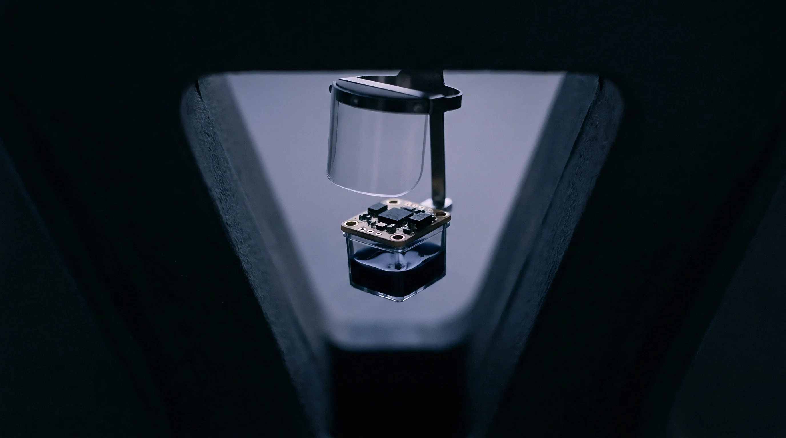

Propagation
Board flexure transfers mechanical energy directly through solder joints into micro-machined silicon die structures. When a printed circuit board bends under chassis fastener torque, thermal expansion, or manual assembly handling, strain moves from the laminate through the interconnect layer into the sensor die. This mechanical coupling shifts the zero-point offset of precision pressure sensors, distorts accelerometer proof-mass anchors, and induces stress-birefringence in optical detector arrays.

Strain Transfer Mechanics across Package Interfaces
Circuit board assembly twisting, enclosure fastener torque, and localized thermal expansion bending induce shear stresses within surface-mount solder interconnects. The strain transmission ratio depends on the mechanical stiffness stack-up between the PCB substrate and the sensor active area. FR-4 laminates exhibit an in-plane flexural modulus between 18 GPa and 24 GPa, whereas monocrystalline silicon possesses a elastic modulus of 130 GPa to 169 GPa along its primary crystallographic axes.
This mechanical impedance mismatch forces solder joints and package substrate materials to absorb flexural strain gradients.
Surface-mount packages transmit board deflection at varying rates based on their physical height, lead geometry, and die-attach elastomer compliance. Rigid Bottom-Terminated Components (BTCs) such as Land Grid Arrays (LGAs) and Quad Flat No-Lead (QFN) packages present low standoff heights between 25 micrometers and 50 micrometers. This short mechanical distance maximizes strain transfer into the die backplate.
Conversely, leaded packages like Small Outline Integrated Circuits (SOIC) or Quad Flat Packages (QFP) utilize gull-wing copper alloy leads that flex elastically, reducing strain coupling by more than 60 percent compared to direct LGA solder attachments.
| Package Format | Solder Standoff Height (µm) | Die-Attach Elastomer Modulus (MPa) | Strain Transmission Ratio (%) | Zero-Point Shift (% Full Scale) |
|---|---|---|---|---|
| LGA-8 (3×3 mm) | 35 ± 10 | 1200 ± 150 | 78 ± 4 | 1.45 ± 0.20 |
| QFN-16 (4×4 mm) | 45 ± 12 | 850 ± 100 | 62 ± 5 | 0.92 ± 0.15 |
| SOIC-8 (Gull-Wing) | 150 ± 25 | 1200 ± 150 | 22 ± 3 | 0.18 ± 0.04 |
| LCC-12 (Ceramic) | 50 ± 15 | 3500 ± 500 | 91 ± 3 | 2.10 ± 0.35 |
Board flex distorts micro-machined diaphragms. The piezoresistive coefficient of silicon translates board-level mechanical strain directly into electrical offset drift. In piezoresistive pressure sensors, a board flexure of 500 microstrain alters the Wheatstone bridge balance, generating zero-point baseline shifts that exceed the intrinsic thermal drift specifications of the sensor element.
- Piezoresistive Bridge Imbalance occurs when differential planar shear strains deform the silicon substrate, altering resistive element values unequally across opposite bridge arms.
- Capacitive Gap Distortion arises when board bending tilts the fixed reference electrode relative to the movable proof-mass in MEMS accelerometers, altering zero-g output voltage.
- Optical Alignment Errors manifest when package flexure rotates internal LED or photodiode dies, shifting optical axis alignment beyond allowable spatial tolerances.
- Die-Attach Delamination accelerates when cyclic shear strain at the substrate interface degrades high-modulus epoxies under thermal shock conditions.
IPC-JEDEC-9704 defines maximum strain thresholds of 500 microstrain for leadless sensor packages, above which zero-point offset stability cannot be contractually guaranteed.
Reflow residual stress settles slowly. The mismatch between the Coefficient of Thermal Expansion (CTE) of the copper traces (17 ppm/K), the FR-4 dielectric (14 to 18 ppm/K), and the silicon sensor die (2.6 ppm/K) locks static strain into solder joints during reflow cooling. This post-reflow stress relaxes over weeks, producing non-linear baseline drift that confounds factory calibration procedures if board-level strain isolation methods are omitted.
Ignoring board-level strain propagation causes sensor calibration failure after final enclosure assembly, forcing expensive recalibration procedures or high field-return rates for uncompensated zero-point offset drift.
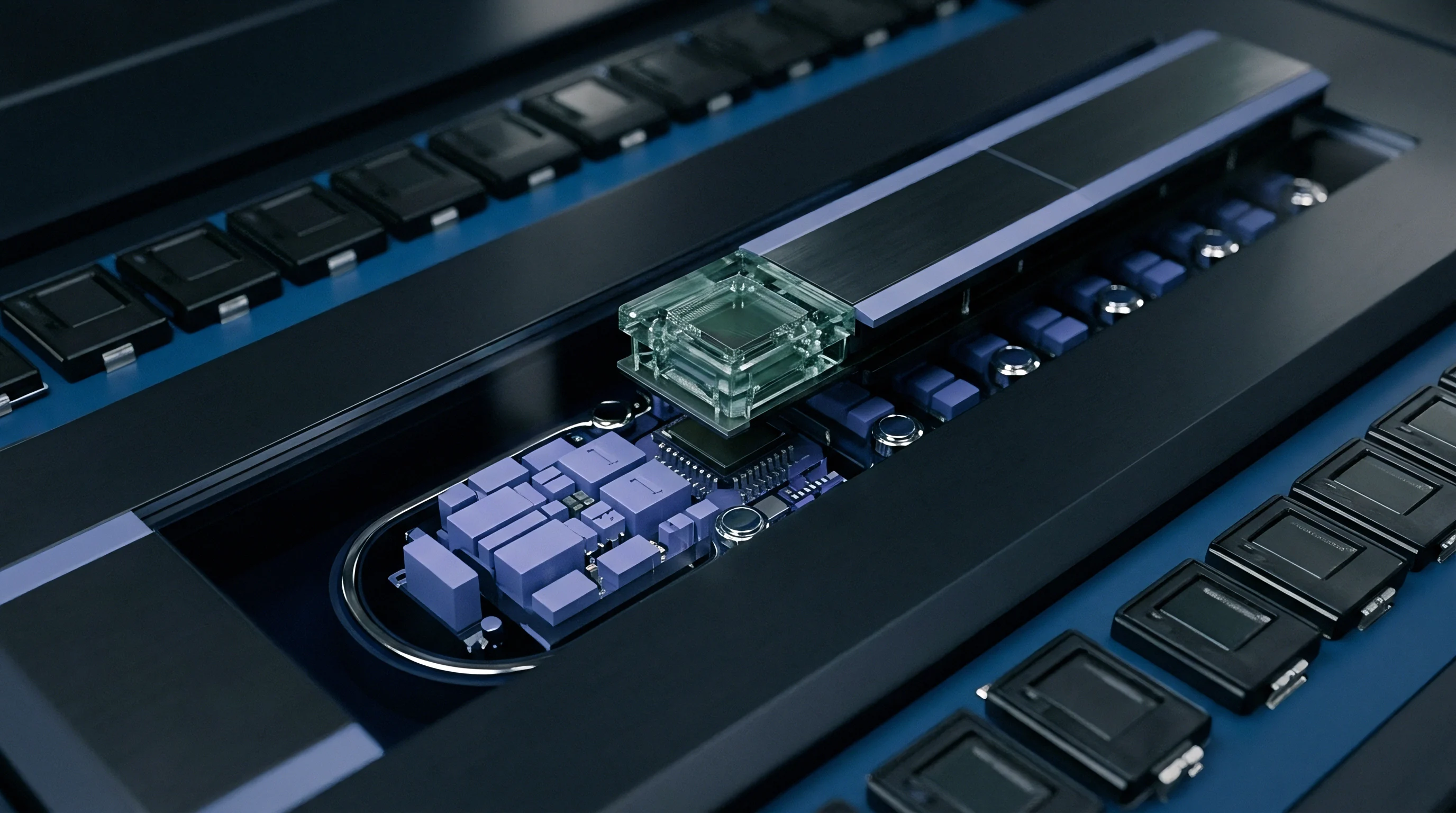

Cutout
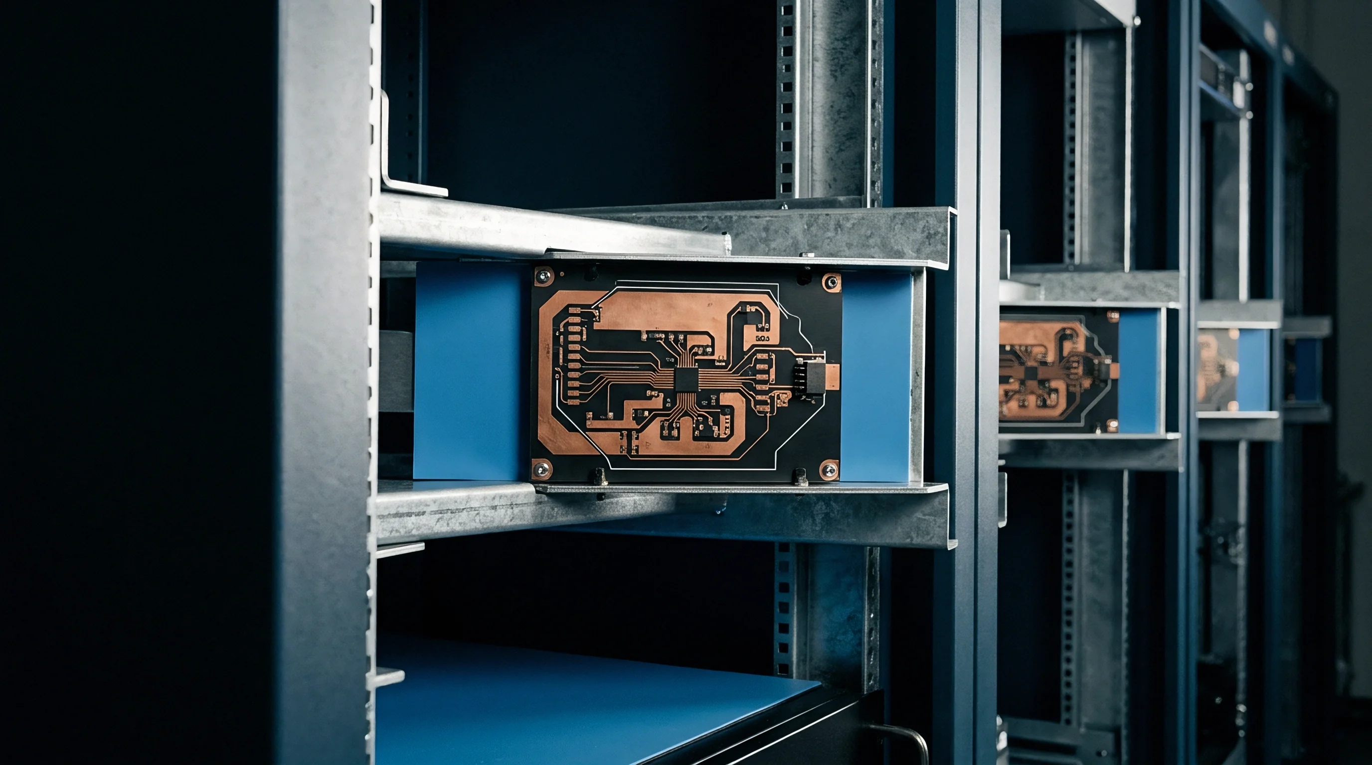
Mechanical isolation through printed circuit board perimeter routing isolates surface-mounted sensor packages from flexural board energy. Machining narrow slots or relief channels directly into the PCB dielectric alters the mechanical load path around the component footprint. This physical separation forces board bending stresses to route through stiff outer board sections, leaving the sensor landing area in a stress-isolated mechanical island.

Board Milling Patterns and Stress Isolation Slots
Routing localized slots around an SMT footprint creates a physical barrier against lateral shear forces. Designers implement U-shaped, C-shaped, or keyhole slot configurations depending on available PCB routing channels and component placement density. A standard dual parallel slot arrangement removes copper and glass-weave material on opposing sides of the sensor package, interrupting mechanical strain transmission lines running perpendicular to the slot axis.
| Isolation Milling Configuration | Slot Width (mm) | Bridge Support Width (mm) | Strain Attenuation (dB) | Island Flexural Rigidity Reduction (%) |
|---|---|---|---|---|
| Dual Parallel Slots | 1.0 ± 0.05 | N/A | -14.2 ± 0.8 | 68 ± 3 |
| Three-Sided U-Slot | 1.2 ± 0.05 | 2.0 ± 0.10 | -21.5 ± 1.1 | 85 ± 2 |
| Keyhole Perimeter Rout | 1.5 ± 0.10 | 1.5 ± 0.10 | -28.4 ± 1.4 | 94 ± 1 |
| Four-Corner Relief Notches | 0.8 ± 0.05 | N/A | -8.6 ± 0.5 | 42 ± 4 |
Slots alter mechanical impedance. By removing structural material adjacent to the sensor footprint, the local stiffness of the board drops dramatically relative to the surrounding motherboard area. Bending moments applied to the primary circuit board deform the narrow supporting webs of the slot structure, protecting the central sensor island from flexure.
- Keepout Zone Radius dictates that no high-mass components or structural mounting screws sit within 5.0 mm of isolation slot bridges to prevent localized stress concentration.
- Trace Routing Constraints limit electrical signal bridges across isolation slots to thin, serpentine traces aligned orthogonally to the mechanical bending axis.
- Milling Width Tolerances specify slot cut accuracy within ±0.05 mm using standard 1.0 mm diameter end-mills to avoid micro-cracks in adjacent inner trace layers.
- Edge Plating Omission requires raw laminate edges inside isolation cuts to remain unplated, preventing rigid copper walls from bridging mechanical strain gaps.
Isolation slot width must exceed maximum board deflection amplitude to prevent mechanical collision between the motherboard and the isolated sensor island during shock loading.
Perimeter milling introduces electrical trace routing challenges. Signals entering the isolated island cross physical support bridges, where bending stresses concentrate. High-density trace routing across these narrow tabs risks mechanical copper work-hardening and fatigue failure under cyclic vibration.
Thicker boards resist deflection, yet require wider routing slots to achieve equivalent mechanical isolation factors.
A narrow isolation slot cut with a worn milling bit leaves glass-fiber micro-burrs that bridge the expansion gap, transmitting board flexure directly across the physical cutout.

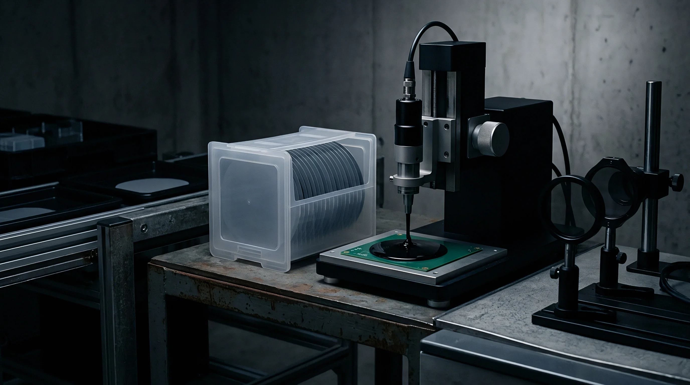
Geometry
Footprint dimensions, pad elevation, and stencil aperture definitions determine the mechanical compliance of solder joints. Solder forms the sole mechanical and electrical interface between the sensor package and the printed circuit substrate. Modifying the landing pad land geometry allows solder joints to deform elastically, reducing the shear stress coupled into the bottom surface of leadless sensor packages.
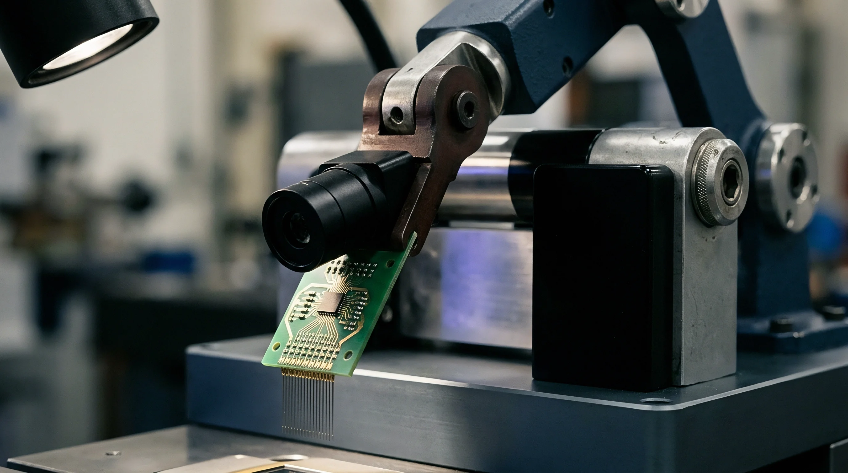
Land Pattern Adjustments and Solder Standoff Mechanics
Increasing solder joint height from 50 micrometers to 150 micrometers decreases shear strain transmission into leadless package bases. The mechanical compliance of a solder joint correlates directly with its aspect ratio, defined as standoff height divided by joint pad diameter. Standard surface-mount processes produce thin, flat joints that exhibit high stiffness in shear mode.
Elevating package standoff creates column-like solder joints capable of bending under board flexure without transferring proportional strain to the die.
- Non-Solder Mask Defined (NSMD) Pad Specification exposes the entire copper pad edge, allowing solder to wet the sidewalls and form a compliant, hourglass-shaped fillet under leadless pads.
- Corner Pad Reduction shrinks the surface area of outer corner pads by 15 percent to 25 percent, mitigating stress spikes that naturally concentrate at package corners.
- Central Thermal Pad Segmenting divides large grounding or thermal pads into an array of smaller, discrete solder lands separated by solder mask webs, preventing rigid center-pad solder sheets.
- Solder Standoff Spacer Placement introduces high-melting-point polymer or micro-sphere spacers into the stencil paste to maintain a controlled minimum solder height during reflow.
Thicker stencil apertures increase solder volume. Elevating joint height requires depositing larger paste volumes without inducing solder bridging between adjacent fine-pitch pads. Stencil design adjustments utilize step-up stencils, increasing aperture thickness from 120 micrometers to 180 micrometers over the sensor footprint area while retaining standard paste heights across the rest of the circuit assembly.
Increasing leadless sensor solder standoff height from 40 micrometers to 120 micrometers reduces board flexure strain transmission into the sensor package by 48 percent under IPC-JEDEC-9704 test conditions.
Leadless packages coupling strain directly require dedicated pad geometry adjustments on multi-layer designs. Thermal expansion gradients between the ceramic sensor base and the organic board substrate strain individual solder columns during environmental thermal cycling. SAC305 solder alloy exhibits creeping behavior under continuous load, leading to solder fatigue cracking if joint compliance is under-engineered.
Purchasing specifications that fail to enforce strict land pattern tolerances risk receiving boards with undersized solder standoff heights, invalidating factory calibration stability limits.

Interposer
Intermediate circuit substrates decouple sensor packages from primary motherboards by absorbing structural deflections. Placing a flexible or semi-rigid carrier element between the sensor package and the main board isolates the die from structural loads. These sub-assemblies translate multi-axis motherboard bending into localized shear deformation within compliant carrier layers.

Why Do Flexible Interposers Shift Zero-Point Calibration Values?
Polyimide film layers and acrylic adhesives undergo moisture absorption and localized creep under sustained ambient humidity. Flexible circuit interposers utilize thin polyimide cores bonded with acrylic or epoxy adhesive systems. Humidity variations alter the physical dimensions and elastic modulus of these adhesive layers, creating mechanical stresses that transfer into the surface-mounted sensor die over time.
This hygroscopic strain produces baseline drift independent of printed circuit board deflection.
| Carrier Architecture | Substrate Construction | Landed Unit Cost Adder (USD) | SMT Assembly Yield Impact (%) | Strain Attenuation Factor (dB) |
|---|---|---|---|---|
| Polyimide Flex Circuit | 50 µm Polyimide + Acrylic Adhesive | 0.45 ± 0.05 | -1.8 ± 0.3 | -32.5 ± 1.2 |
| BT-Epoxy Rigid Subboard | 0.4 mm BT-Laminate (High-Tg) | 0.28 ± 0.03 | -0.4 ± 0.1 | -18.2 ± 0.9 |
| Coin-on-Board Copper Tab | Stamped Alloy C19400 Leadframe | 0.62 ± 0.08 | -2.5 ± 0.4 | -24.1 ± 1.0 |
| Elastomeric Interposer Socket | Silicone Matrix + Conductive Columns | 1.15 ± 0.12 | -0.1 ± 0.05 | -36.0 ± 1.5 |
Interposers add thickness. Integrating a secondary substrate layer increases the overall assembly height by 0.3 mm to 1.2 mm, restricting usage in space-constrained mobile or wearable applications. Furthermore, secondary reflow or hand-soldering operations required to attach interposers introduce yield risks during volume manufacturing.
Component suppliers frequently explain baseline offset drift by claiming board assembly processes exceeded recommended thermal ramp rates, ignoring the inherent stress transmission of their rigid LGA footprints.


Encapsulation
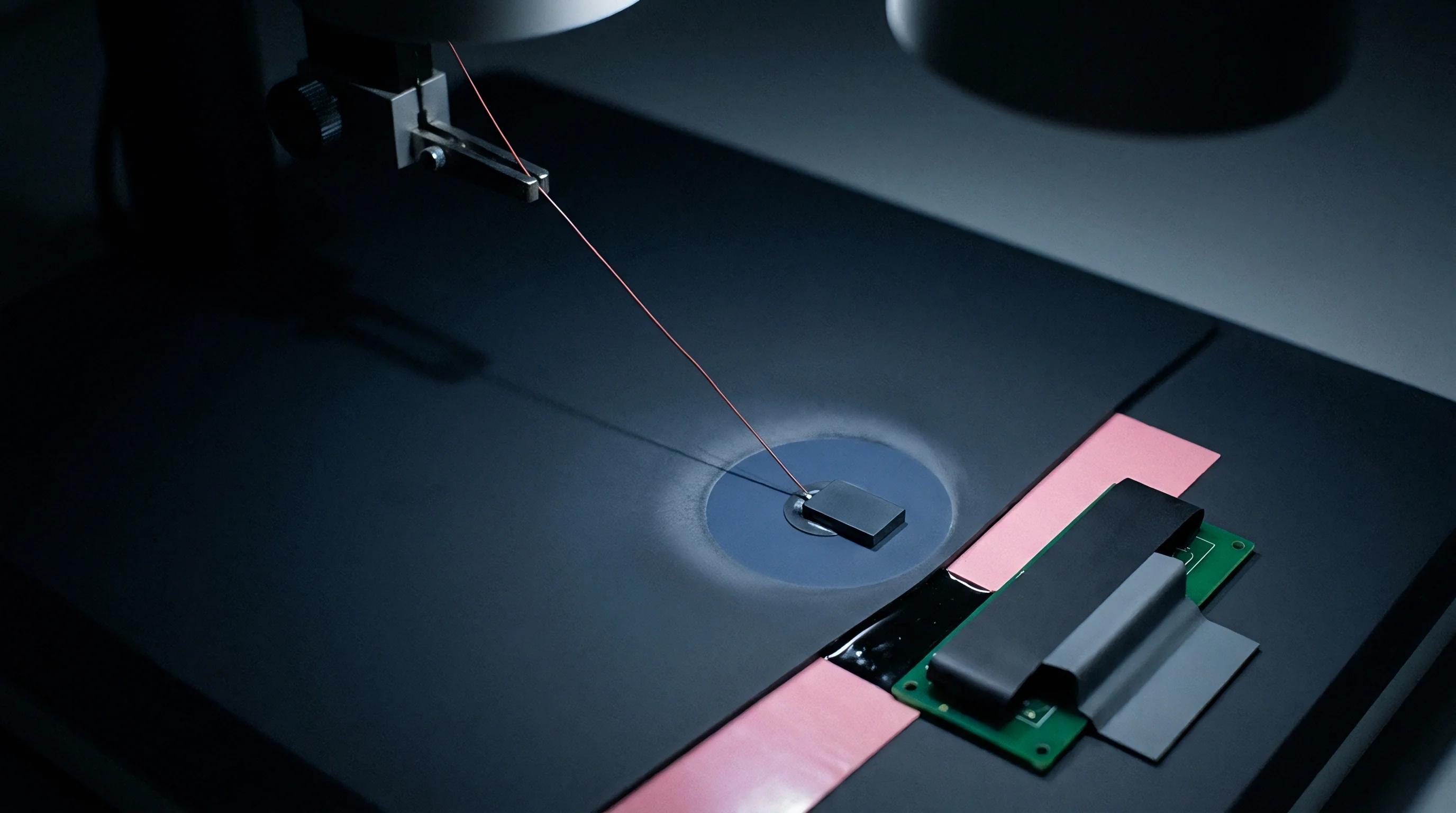
Compliance coatings and low-modulus potting compounds damp environmental vibrations while decoupling package surfaces. Applying soft silicone gels or specialized elastomer encapsulants around mounted sensor dies creates a shock-absorbing envelope. This protective gel layer isolates sensitive sensing elements from external mechanical stress without restricting intentional physical inputs such as ambient pressure changes.
Gel Buffers and Soft Media Isolation
Silicone gels with Shore 00 hardness ratings under 30 isolate pressure diaphragms without imparting thermal expansion forces. High-modulus epoxies or rigid glob-top resins contract strongly during polymerization, locking compressive stresses into the sensor die surface. Low-modulus silicone gels maintain compliance across wide temperature ranges, providing environmental protection against moisture while buffering mechanical shock.
Gel compliance drops at low temperatures. As ambient conditions approach the glass transition temperature of the silicone material, the gel modulus increases by several orders of magnitude. Below minus 40 degrees Celsius, previously soft gel encapsulants turn rigid, transmitting board-level strain and internal thermal expansion forces directly into the sensor die diaphragm.
- Material Specification Document defining the gel Young’s modulus below 1.0 MPa and glass transition temperature below minus 50 degrees Celsius.
- Dispense Volume Control Limits mandating automated weight verification within ±2.0 milligrams to maintain constant gel height over the die surface.
- Thermal Cure Profile Record documenting peak curing temperature and ramp rates to eliminate void formation and residual curing strain.
- Outgassing Verification Report certifying compliance with ASTM E595 Total Mass Loss limits below 1.0 percent.
Silicone gel potting with a Young’s modulus below 500 kPa attenuates high-frequency mechanical vibration by more than 20 dB while transmitting less than 2 percent of substrate flexure to the sensor diaphragm.
Potted sensors require low-modulus gels. Standard conformal coatings like acrylics or polyurethanes possess moduli above 100 MPa, rendering them too rigid for strain-sensitive MEMS applications. Selecting an inappropriate gel formulation negates the strain isolation benefits achieved through PCB slotting or specialized land patterns.
Does the low-temperature gel stiffening phenomenon induce unrecoverable zero-point offset shifts during cryogenic thermal storage cycles?

Yield
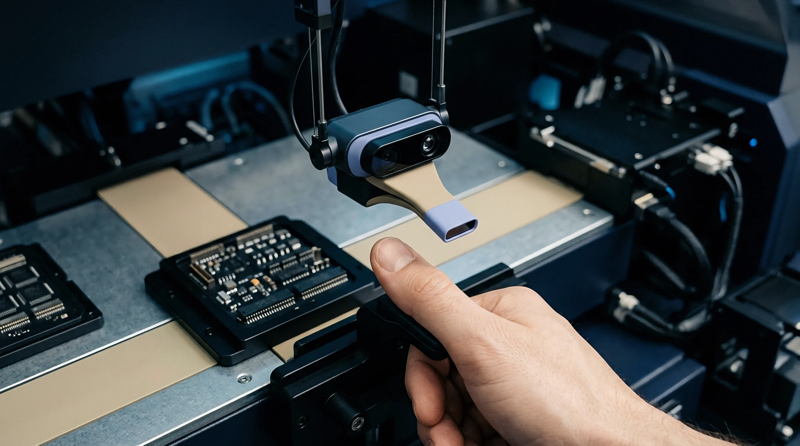
Production efficiency relies on balancing mechanical strain attenuation against total manufacturing cost per placement. Selecting high-performance strain decoupling techniques increases raw bill-of-materials expenses, adds SMT processing steps, and alters board-level inspection metrics. Sourcing practices evaluate mechanical strain isolation methods by quantifying unit cost increases against field failure risk reduction.

Strain Budget Verification and Landed Unit Arithmetic
Strain gauge rosette testing verifies board flexure during panel singulation, connector insertion, and final enclosure assembly. Placing triaxial strain gauge rosettes at high-risk sensor footprints identifies peak mechanical strain vectors generated during manufacturing. If measured strain values exceed 500 microstrain, process modifications or layout isolation structures must be implemented to protect production yield.
Implementing perimeter routing slots represents an inexpensive strain isolation method, requiring no additional components on the bill of materials. However, isolation slots consume valuable PCB routing real estate and increase panel routing time at the board fabricator, adding approximately 0.03 USD to 0.08 USD per panel. In high-density layouts where routing channels cannot accommodate perimeter cuts, engineers must select discrete interposers or elevated land geometries, shifting costs directly onto component procurement budgets.
Solder height absorbs flexure. Modifying stencil apertures and pad land patterns incurs zero ongoing unit material costs, making footprint optimization the most commercially efficient first-line defense against strain-induced sensor offsets. Take a 100,000-unit production run comparing three strain isolation approaches:
Direct QFN mounting with standard 35 micrometer standoff requires no added material cost, but experiences a 2.5 percent yield loss at final test due to zero-point offset drift caused by reflow thermal strain. The cost of scrapped assemblies at 12.00 USD per populated board totals 30,000 USD across the build.
Implementing board isolation slotting adds a 0.05 USD PCB fabrication charge per board, totaling 5,000 USD. Scrapped units drop to 0.2 percent due to mechanical isolation, resulting in 2,400 USD in test scrap costs. The net savings achieved by milling isolation slots equals 22,600 USD per 100,000 units produced.
Adopting a pre-assembled flexible interposer adds 0.45 USD per sensor footprint in component cost and assembly overhead, totaling 45,000 USD. Scrap drops to near zero (0.05 percent), costing 600 USD in scrap. Total implementation cost equals 45,600 USD, presenting a net loss compared to simple board milling unless board routing density makes slots physically impossible.
Assembly yield drops without relief notches. High-volume manufacturing lines require repeatable land pattern designs and verified strain isolation parameters to maintain profitability. Sourcing decisions must align mechanical performance requirements with clear landed-cost calculations prior to schematic freeze.