Polymeric Underfill Selection for Flip Chip Sensor Reliability
Polymeric underfill selection balances thermomechanical bump fatigue isolation against die strain output drift, process flow speed, and landed unit yield costs.
Stress
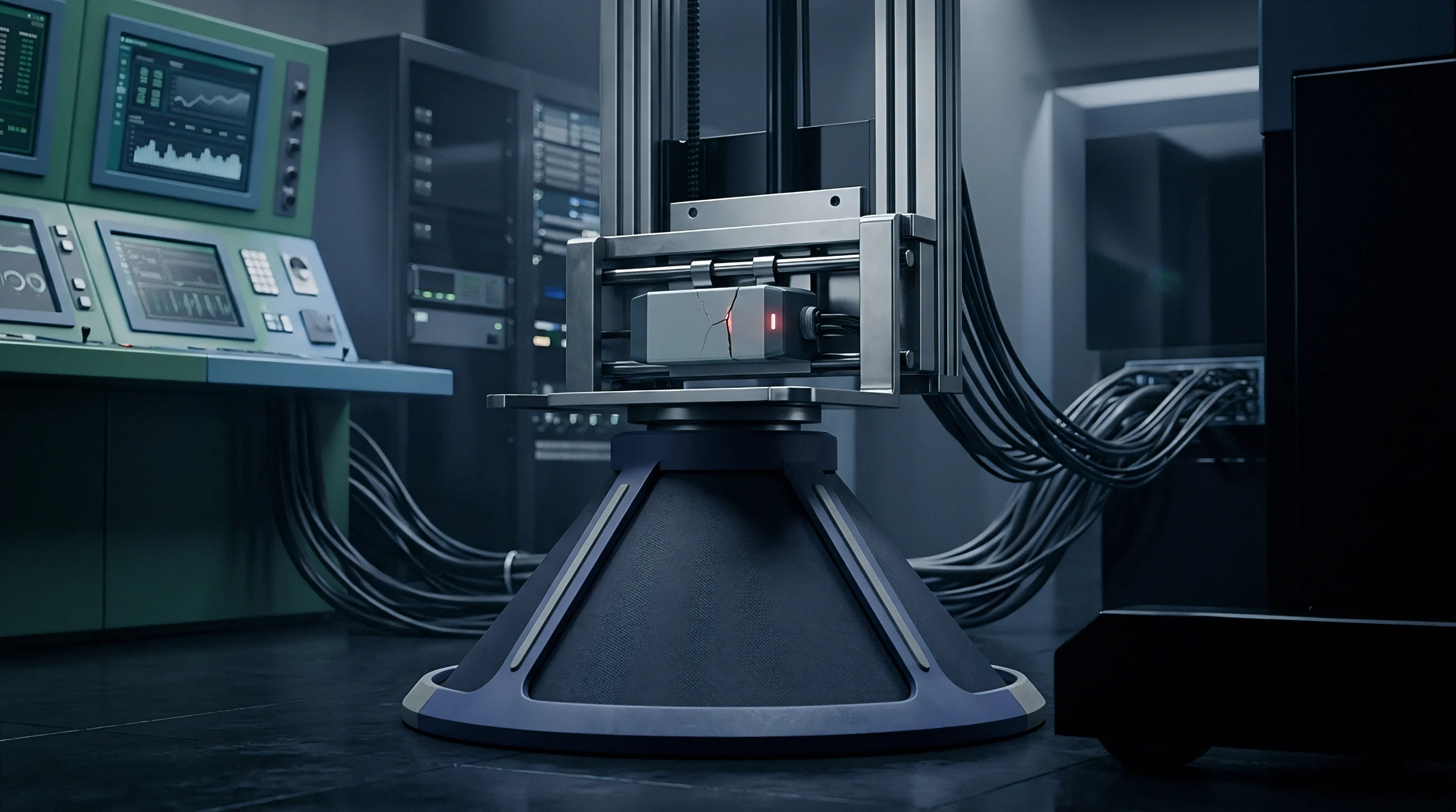
Flip chip mounting transfers thermal strain directly into silicon, mechanically linking a die with a coefficient of thermal expansion near 2.6 ppm/K to an FR-4 organic substrate that expands at 14 to 17 ppm/K. Thermal cycling forces the solder interconnects to absorb this expansion mismatch through plastic shear strain. In unfilled flip chip assemblies, corner bumps fail rapidly from fatigue where distance from the neutral point peaks.
Polymeric underfill redistributes this thermal mismatch across the die surface. Encapsulating the solder bumps in a rigid epoxy matrix shifts stress off individual interconnects and into the bulk die and substrate composite. This structural coupling alters the mechanical state of the sensor die: axial and shear stresses from underfill cure shrinkage distort physical elements inside microelectromechanical systems and piezoresistive sensor architectures.
That mechanical stress modifies the silicon band structure, shifting piezoresistance coefficients and producing output drift in differential pressure and force sensors.
| Interconnect Configuration | Pitch (µm) | Stand-off Height (µm) | Unfilled Fatigue Life (Cycles to 1% Failure) | Underfilled Fatigue Life (Cycles to 1% Failure) | Piezoresistive Offset Shift post-Cure (mV/V) |
|---|---|---|---|---|---|
| 180 ± 5 | 85 ± 4 | 220 | 3800 | 0.85 ± 0.12 | |
| 150 ± 4 | 65 ± 3 | 140 | 2900 | 1.42 ± 0.18 | |
| 80 ± 2 | 35 ± 2 | 45 | 2200 | 2.15 ± 0.25 | |
| 200 ± 5 | 95 ± 5 | 310 | 4500 | 0.62 ± 0.08 |
Die thickness directly governs mechanical rigidity under cure strain. Thinning silicon dies below 150 µm lowers bending stiffness, allowing underfill epoxy to warp the package into a concave or convex profile depending on thermal history. Optical sensor arrays mounted with flip chip interconnects suffer spatial pixel mispointing when underfill fillet height varies along opposing die edges; unbalanced dispense fillets generate asymmetric bending moments that can shift optical focal planes by up to 12 arcminutes across standard manufacturing thermal windows.
A high-modulus capillary underfill cured at 150°C introduces over 120 MPa of compressive planar stress into a 100 µm thick sensor die at room temperature.
Piezoresistive bridge outputs reflect structural package stress. Compressive stress acting on p-type silicon piezoresistors induces non-linear offset shifts that override active thermal compensation networks in sensor signal conditioners. MEMS pressure sensor diaphragms mounted via flip chip interconnects undergo baseline offset changes when underfill spills onto active diaphragm regions or creates asymmetric stress fields near anchor points.
Choosing an underfill with excessive elastic modulus or high volumetric shrinkage leads directly to unrecoverable zero-point offset errors beyond on-chip digital trim ranges.

Chemistry
Polymeric underfill formulations consist of thermosetting resin blends, hardeners, catalysts, dynamic coupling agents, and inorganic filler particles. Epoxy resin systems based on bisphenol-A, bisphenol-F, or cycloaliphatic structures form the cross-linked matrix. Adding fused spherical silica particles lowers the effective coefficient of thermal expansion from 65 ppm/K toward the 20 ppm/K target of solder bumps while raising the elastic modulus from 2.5 GPa to over 10 GPa.
Glass transition temperature dictates low-stress operation. Below this transition point, the cured polymer remains rigid with a low coefficient of thermal expansion (CTE1). Above it, the matrix softens into CTE2, expanding at three to four times the rate of CTE1.
Thermomechanical reliability requires a glass transition temperature that stays above the sensor assembly’s maximum continuous operating temperature.
- Capillary Underfill Epoxies rely on low initial liquid viscosity below 0.3 Pascal-seconds at dispense temperature to draw fluid into low-clearance die gaps using capillary action.
- Non-Conductive Film Polymers arrive pre-applied on sensor wafers, requiring precise thermal compression bonding tools to melt the film and make interconnect contact simultaneously.
- No-Flow Underfill Resins apply directly onto substrates prior to die placement, combining fluxing chemistry with structural resin matrix that cures during standard surface-mount reflow profiles.
- Wafer-Level Liquid Underfills cover the entire active face of wafer assemblies before dicing, leaving cured material along bump flanks to isolate individual interconnect structures.
Particle size distribution governs flow capability through tight gaps. Fused silica filler grains must keep their maximum particle diameter below one-third of the minimum bump stand-off clearance to prevent bridging and flow blockage. A 30 µm bump gap demands underfill formulations with a maximum particle diameter under 10 µm and an average diameter centered near 2 µm.
Filler settling during thermal cure creates vertical resin gradients, leaving an unfilled resin-rich layer near the die surface with poor thermomechanical stability.
Silica filler particle size exceeding one-third of the solder bump stand-off height causes physical flow blockage and localized void clusters during capillary dispense cycles.
Polymer cure kinetics establish structural cross-link density. Fast-curing snap formulations achieve full polymerization inside 90 seconds at 165°C, reducing manufacturing cycle times on high-volume assembly lines. These rapid cross-linking reactions build higher internal stress states than extended profile ovens that ramp temperature across 30 minutes.
Published datasheet modulus numbers apply only to fully relaxed test specimens cured under laboratory convection conditions.

Process
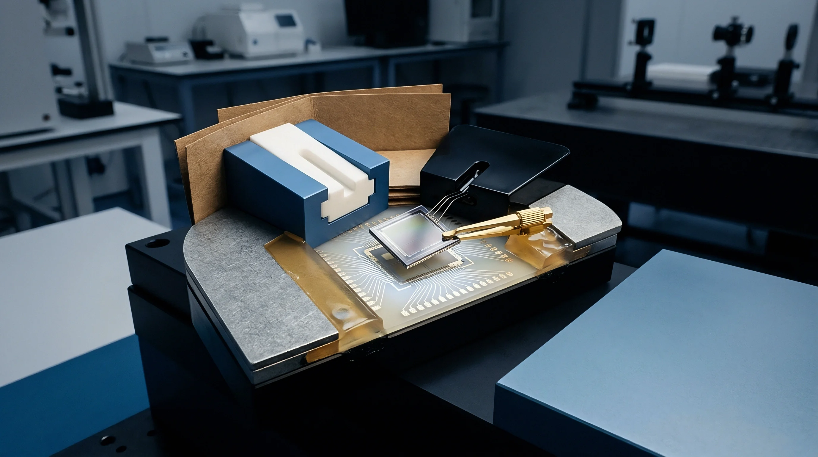
Dispensing underfill demands tight thermal and volumetric fluid control. Substrate heating panels maintain assembly temperatures between 70°C and 110°C to lower capillary underfill viscosity without initiating premature cross-linking inside the dispensing needle. Precision positive displacement pumps trace single-line, L-shape, or U-shape paths adjacent to die edges.
Capillary flow relies on surface energy. Wetting dynamics force fluid through the array gap, displacing air until liquid emerges along opposing die boundaries.

Can Underfill Fillet Height Shift Sensor Zero-Point Offset?
Fillet profile geometry establishes mechanical boundary conditions along die edges. Over-dispensing underfill forms a high fillet that climbs the silicon die sidewall, contacting top-surface passivation and transferring stress into sensitive sensor layout zones. Conversely, low fillets expose corner solder bumps to moisture ingression and local mechanical fatigue.
Asymmetric fillets generate uneven torque across the die face, shifting zero-point output levels on integrated force and MEMS acceleration sensors.
| Preheat Temperature (°C) | Dispense Pattern | Gap Flow Velocity (mm/s) | Acoustic Void Detection Rate (%) | JESD22-A104 Cycle Life (-40°C to 125°C) |
|---|---|---|---|---|
| 0.45 ± 0.05 | 4.2 | 1800 | ||
| 1.25 ± 0.08 | 0.1 | 3400 | ||
| 1.18 ± 0.07 | 8.6 | 950 | ||
| 2.10 ± 0.12 | 1.8 | 2200 |
Void formation during capillary flow degrades thermomechanical isolation. Trapped moisture inside unvented voids expands rapidly during high-temperature reflow or environmental exposure, initiating delamination cracks along the epoxy-silicon passivation interface. Multi-pass dispensing on adjacent die sides captures air bubbles where fluid fronts meet from perpendicular directions.
Single-edge dispensing allows one uniform liquid front to sweep across the bump array, pushing trapped gas toward open edges.
Curing schedules lock in stress states. Substrate processing specifications require scanning acoustic microscopy to inspect assemblies post-cure. Standard acceptance under IPC-A-610 rejects underfilled sensor packages exhibiting delamination along die corners or voiding across more than 10 percent of total die area.
- Preheat substrate carrier plates on the automated inline dispense system to 85°C with a tolerance of ± 3°C.
- Purge positive displacement valve needles and verify volumetric discharge accuracy to within ± 2 percent by weight.
- Execute a single-line dispense pass parallel to the longest die edge at a standoff height equal to half the needle inner diameter.
- Pause movement for 15 seconds to allow complete capillary flow across the die width before inspecting leading-edge fillet emergence.
- Transfer assemblies to a forced-convection curing oven running a programmed temperature ramp of 5°C per minute up to 150°C.
- Hold the peak curing temperature of 150°C for 45 minutes before cooling assemblies to ambient line conditions.
Underfill voiding covering more than 10 percent of total die surface area invalidates thermal cycling compliance under AEC-Q100 Grade 1 qualification rules.
Tuning inline fluid dispensing involves persistent trade-offs. High substrate temperatures lower fluid viscosity and speed up flow across dense bump fields, but excessive thermal exposure accelerates gelation before the gap fills completely. Lower preheat settings prevent premature gelling yet extend flow duration past economical SMT line beat times.
Finding the optimum fluid kinetic window across batch-to-batch viscosity variations remains a constant line optimization challenge.

Bus
Mechanical strain from cured underfill modifies transducer outputs, forcing digital compensation algorithms to expand calibration correction factors. Integrated MEMS and piezoresistive die architectures convert force, pressure, or acceleration into electrical signals using balanced bridge structures. While equalized strain distributions preserve zero-point offsets, asymmetric underfill stress shifts bridge balance, introducing a baseline offset error before any physical input reaches the device.
Firmware teams manage package strain by reading sensor registers across multi-point thermal calibration cycles. Standard factory trim routines write digital offset correction coefficients into non-volatile memory or EEPROM registers via I2C or SPI interfaces during final test. Nonlinearities in underfill thermal expansion alter second-order temperature coefficient profiles, requiring higher-order polynomial calculations inside the host microcontroller to maintain accuracy across operating temperatures.
- Offset Value Tracking monitors raw sensor output registers prior to underfill dispense, post dispense, and following full oven cure to calculate net mechanical strain.
- Gain Drift Correction recalculates full-scale output multipliers to adjust for piezoresistive sensitivity reduction induced by bulk die compressive stress.
- Polynomial Order Escalation upgrades firmware thermal compensation equations from linear to quadratic forms when underfill transition behavior introduces curvature into register readings.
- EEPROM Burn Operations commit post-assembly strain offset corrections into internal sensor registers over standard serial communication lines.
Bus communication integrity relies on stable internal voltage reference levels. Package warpage induced by low-Tg underfills shifts bandgap reference voltages inside the analog front-end die, introducing system-wide gain errors across analog-to-digital converter channels. SPI clock frequencies up to 10 MHz allow fast readout of uncompensated register values, enabling host processors to run dynamic software filtering routines when hardware registers run out of trim range.
Firmware offset tables cannot fix hysteresis.
Viscoelastic relaxation of cured underfill resins causes baseline sensor register drift over 500 operating hours that software calibration curves cannot anticipate.
Underfill mechanical creep creates long-term output instability. Cured epoxy matrices undergo viscoelastic relaxation over extended thermal exposure, altering die stress states over months in the field. Dynamic calibration routines programmed into host firmware must continuously track baseline output drift to separate genuine environmental signal changes from underfill relaxation.
Formulations with high glass transition temperatures and low creep compliance minimize register offset drift over product operational lifespans.
Ledger
Evaluating underfill options demands an integrated analysis of silicon packaging costs, surface-mount assembly throughput, yield impacts, and capital expenditure amortization. A bare flip chip die purchased on tape and reel represents the lowest initial component cost, but processing it requires dedicated dispensing equipment, acoustic inspection systems, and extended thermal curing ovens. Pre-applied Non-Conductive Film or wafer-level underfill packaging options increase initial die costs while eliminating inline dispense machinery and fluid flow dwell times.
Yield losses escalate rapidly. Inline capillary dispensing failures lead directly to scrapped assemblies containing fully populated, high-value printed circuit boards. A single unvetted fluid batch exhibiting premature gelation can ruin an entire production run before acoustic micro-imaging flags under-die voiding.
Yield calculations must balance the unit price premium of wafer-level underfill processing against board-level scrap rates associated with capillary fluid dispensing operations.
Consider a practical manufacturing worked construction comparing Capillary Underfill against pre-applied Non-Conductive Film across a high-volume automotive sensor run. Assume a baseline volume of 500,000 units annually utilizing a 5 mm by 5 mm flip chip pressure sensor die with 120 SAC305 bumps on an 80 µm pitch. The bare die costs $1.85 in tape-and-reel format.
Equipping an SMT line with an inline dual-head fluid dispenser, substrate preheat station, and forced-convection curing oven adds $220,000 in capital outlay, amortized across three years at $73,333 annually, yielding a fixed equipment cost of $0.147 per unit.
Capillary underfill fluid costs $420 per 30 cc syringe, dispensing 0.04 cc per sensor die, yielding 750 parts per syringe for a direct fluid material cost of $0.560 per unit. Inline capillary flow dwell time reduces total SMT line placement speed by 1.8 seconds per board, adding $0.035 in variable machine time costs. Capillary dispensing yield loss sits at 1.2 percent on finished boards valued at $12.00, introducing an expected scrap cost of $0.144 per unit.
The fully landed assembly contribution for capillary underfill totals $0.886 per unit above bare die costs, producing a net manufactured cost of $2.736 per unit.
Procuring the same sensor die with pre-applied Non-Conductive Film increases component cost from $1.85 to $2.60 per unit. Non-Conductive Film eliminates inline fluid dispensing systems, capillary flow pauses, fluid waste, and underfill cure ovens, while requiring a thermo-compression die bonder addition costing $180,000, amortized over three years at $60,000 annually, yielding $0.120 per unit fixed capital cost. Scrap rates drop to 0.2 percent due to automated film thickness control during wafer processing, contributing $0.024 per unit in expected scrap losses.
Fully landed assembly contribution for pre-applied film totals $0.144 per unit above wafer component costs, yielding a net manufactured cost of $2.744 per unit.
At 500,000 units per year, capillary dispensing offers a slim $0.008 per unit advantage over pre-applied film options. Crossing a volume threshold of 750,000 units annually shifts economic preference toward capillary underfill due to lower component premiums on bare silicon die. Lower production runs below 200,000 units per year favor pre-applied film formats, avoiding inline fluid dispensing equipment investments and complex capillary fluid handling logistics on short assembly lines.
Sourcing agreements specify strict lot acceptance parameters for polymeric underfill shipments. Procurement contracts enforce JEDEC J-STD-020 reflow survival guarantees, requiring underfill suppliers to replace full material batches if resin viscosity varies by more than 10 percent from baseline specification sheets during incoming quality verification testing.