Material System
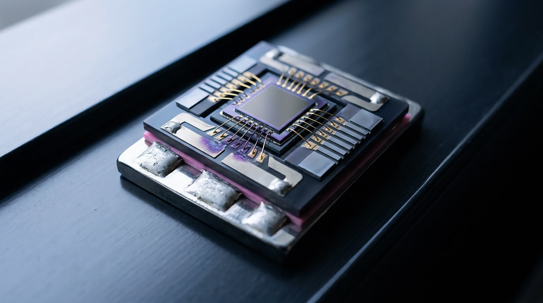
Adhesive sheets without conductive filler particles protect high-density microelectronic interconnects from environmental and mechanical damage. Utilizing non conductive film provides both a physical barrier and structural reinforcement between the chip and the substrate during the bonding process. This material is designed to flow under heat and pressure before curing into a rigid solid.
Assembly Procedure
Thermocompression bonding is the standard technique for applying this adhesive material during chip attachment. When the non conductive film is compressed, it is squeezed out from the contact area, which allows the gold or copper bumps to make direct metal-to-metal connection. The adhesive then fills the remaining voids between the chip and the substrate to form a solid encapsulating layer.
Reliability Benefit
Encapsulation of the joint prevents moisture ingress and solder bridging under harsh operational environments. The cured non conductive film also reduces the stress on individual contacts by distributing mechanical loads across the entire die area. This reduction in localized stress extends the life of fine-pitch assemblies.
Process Constraint
Moisture absorption in the uncured material can cause voiding or delamination during high-temperature reflow cycles. Ensuring proper storage in dry conditions is therefore necessary to maintain the integrity of the adhesive joint before the final cure. Any moisture trapped in the film expands rapidly during solder reflow, which can rupture the delicate connection between the microelectronic package and the board, resulting in expensive repair or product scrap.