Parasitic Lead Reactance Effects in Precision Semiconductor Enclosures
Package lead parasitics induce ground bounce and high-frequency ringing; migrating to leadless formats reduces lead inductance below 0.5 nH per terminal.

Frame
Precision semiconductor die require a physical structural matrix to bridge microscopic silicon bond pads to circuit board land patterns. Metallic leadframes, ceramic carriers, and bond wires provide mechanical enclosure and environmental protection, yet each millimeter of conductive path introduces unintended electric and magnetic energy storage. Metallic leads act as distributed transmission lines with non-zero self-inductance, pin-to-pin parasitic capacitance, and series resistance.
Bond wire length dominates.
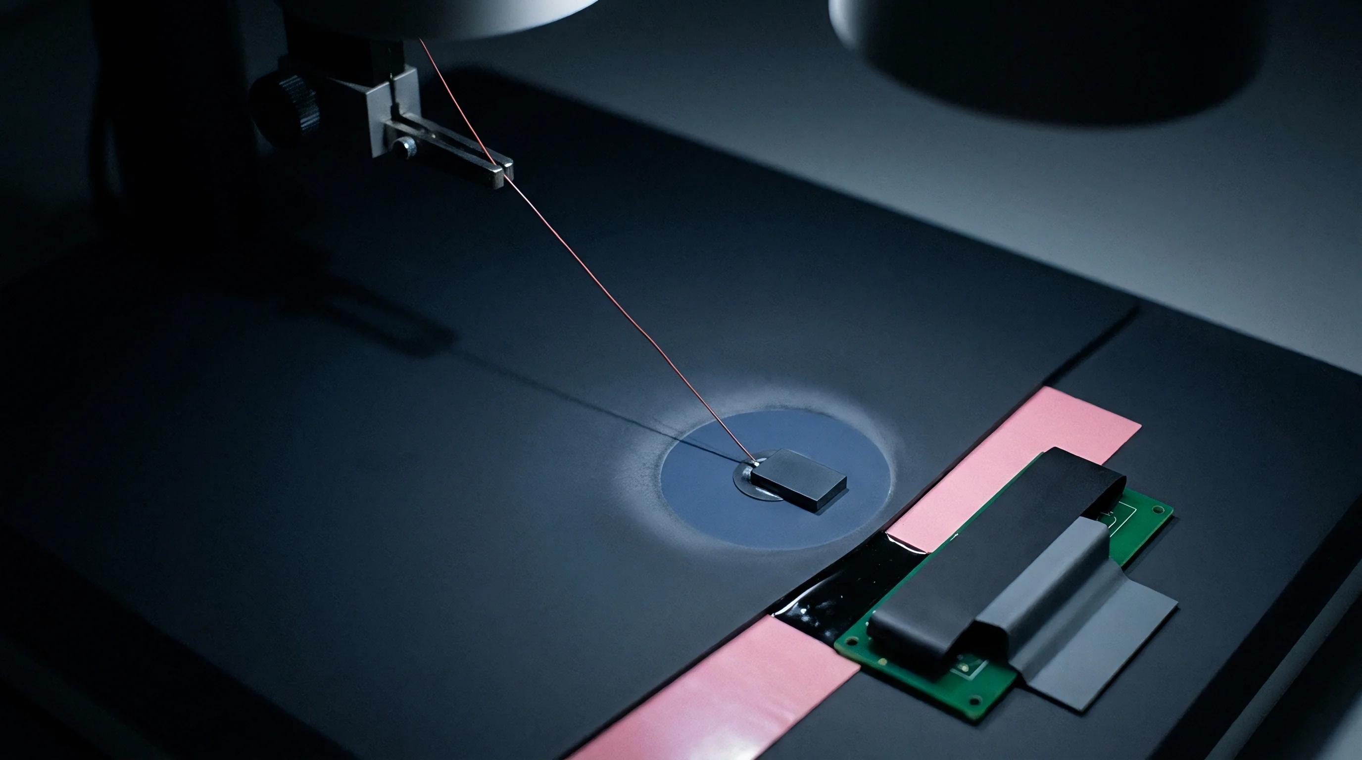
Standard leadframe materials such as Copper Alloy C194 or Iron-Nickel Alloy 42 present intrinsic electrical properties that scale with mechanical dimensions. Partial self-inductance inside a packaged integrated circuit stems primarily from the thin internal lead traces and fine gold or copper wire bonds bridging the die to the leadframe paddle. A straight conductive pin carries a partial self-inductance determined by its length, width, and cross-sectional thickness.
Expressed analytically, partial self-inductance scales directly with conductor length and logarithmically with the ratio of length to cross-sectional perimeter.

Leadframe Conductor Geometry
Every millimeter of internal conductor track adds approximately 0.6 nH to 1.2 nH of series inductance, depending on the trace profile and height above the package metal paddle. In a surface-mount Small Outline Integrated Circuit (SOIC) package, an outer pin combined with its internal leadframe finger stretches over 3.5 mm in length. Wire bonds contribute an additional 0.8 nH to 1.5 nH per millimeter, depending on loop height and wire diameter.
A standard 25-micrometer gold bond wire suspended 200 micrometers above a die paddle forms a inductive loop that degrades high-frequency current delivery.
A 1.27 mm pitch SOIC lead frame contributes approximately 1.8 nH of self-inductance per pin at 100 MHz operating frequency.
Pin-to-pin capacitance develops across the narrow insulating gaps separating parallel package leads. Mold compound dielectric constants typically range from 3.5 to 4.2 at room temperature. Thin air-filled or resin-filled spaces between pins yield inter-lead capacitance values between 0.2 pF and 0.8 pF for standard 0.65 mm and 1.27 mm lead pitches.
High-density pinouts compress conductor spacing, elevating shunt capacitance and facilitating high-frequency crosstalk between adjacent signal lines.
Mutual Inductive and Capacitive Coupling
Current transitions through a single lead induce voltage spikes in neighboring conductors through mutual magnetic coupling. Electromagnetic field overlap between parallel leadframe fingers creates mutual inductance values reaching 20 to 35 percent of the pin self-inductance. When high-speed digital interface lines switch simultaneously, mutual inductance couples switching noise directly into sensitive analog bias pins sharing the same leadframe side.
Physical symmetry inside plastic mold compounds does not guarantee electrical symmetry. Corner pins in Quad Flat Package (QFP) configurations trace significantly longer physical paths than center pins. A corner lead in an 80-pin QFP exhibits up to 70 percent higher series self-inductance compared to a center lead on the same edge.
Designing high-precision differential amplifiers or low-noise voltage references without accounting for pin position bias guarantees asymmetrical signal propagation delays and common-mode rejection breakdown.
Ignoring package lead parasitic reactance during preliminary schematic design yields unexpected analog offset errors, thermal calibration drift, and signal degradation that invalidates system performance specifications late in the hardware build cycle.

Distortion
Dynamic signal currents traversing parasitic package inductors generate transient voltage drops according to Faraday’s law of induction. Rapid variations in current over time induce instantaneous potential differences across power supply leads and ground return paths. Ground bounce destroys precision.
Ground bounce occurs when simultaneous switching of digital output drivers forces rapid current discharge through shared package ground pins. The parasitic series inductance of the ground lead suppresses instantaneous current flow, causing the internal die ground reference to shift relative to the external system ground. An internal ground rail displacement as small as 50 mV alters the switching thresholds of input logic gates and corrupts analog-to-digital converter conversions.

Package Failure Modes
Parasitic reactance within precision enclosures initiates distinct physical and functional failure mechanisms across analog and mixed-signal domains.
- Ground Bounce Phase Shift ~ Transient voltage displacement across package return pins shifts internal analog ground references, introducing dynamic DC offset errors in high-resolution signal chains.
- LC Ringing and Overshoot ~ Ringing triggers false digital clock edges when parasitic lead inductance resonates with internal gate input capacitance.
- Bandwidth Attenuation Roll-Off ~ High-frequency operational amplifier gain rolls off prematurely due to low-pass filtering formed by lead self-inductance and trace capacitance.
- Power Supply Rail Sag ~ Instantaneous current demands induce supply voltage drops across package power pins, degrading operational amplifier power supply rejection ratio performance.
- Crosstalk Injection Noise ~ Fast-edge digital interface signals couple switching energy into neighboring high-impedance sensor inputs via mutual pin-to-pin capacitance.

Settling Time Expansion
High-precision instrumentation amplifiers require fast, clean step responses to settle within specified accuracy windows. Lead reactance creates high-Q resonant circuits when paired with die pad capacitances and board trace capacitance. Undamped resonance produces damped high-frequency ringing on transient step edges.
Settling time expands by microseconds.
Exceeding the maximum pin inductance threshold specified under JEDEC JESD22-B111 invalidates high-speed signal integrity guarantees.
Linear signal paths suffer from phase margin erosion when parasitic inductance sits in series with low-impedance feedback nodes. An operational amplifier driving an external load through a high-inductance package lead experiences an additional pole in its open-loop frequency response. Phase margin drops rapidly.
Undesired feedback loop instability follows, turning precision gain stages into uncontrolled RF oscillators.
Suppliers frequently defend unexpected offset drift and high-frequency gain peaking by attributing signal distortion to improper board-level decoupling rather than acknowledging intrinsic leadframe parasitic boundaries.

Package
Selecting an enclosure format balances mechanical robustness, board assembly yields, and electrical parasitic performance. Traditional leaded packages offer inspectable solder joints and high thermal stress tolerance, yet their elongated metallic leads introduce severe inductive penalties. Leadless bottom-terminated components reduce package lead length to sub-millimeter scales, suppressing parasitic reactance at the expense of higher board assembly precision requirements.

Why Do QFN Package Transitions Shift Analog DC Calibration?
Transitioning a precision analog die from a Dual In-line Package (DIP) or Small Outline (SOIC) package to a Quad Flat No-Lead (QFN) format drastically compresses physical lead length. The eliminate of external Gull-Wing pins reduces series lead inductance from 3.5 nH down to 0.5 nH per terminal. Internal wire bond paths are shortened or replaced entirely by flip-chip solder bumps.
Parasitic capacitive coupling between adjacent contacts drops proportionally as terminal surface areas shrink.
| Package Format | Pin Inductance (nH) | Pin Capacitance (pF) | Bandwidth Limit (MHz) | Footprint Area (mm²) |
|---|---|---|---|---|
| TO-39 Metal Can | 6.5 ± 0.8 | 1.2 ± 0.2 | 45 | 70.8 |
| SOIC-8 Plastic | 2.1 ± 0.3 | 0.6 ± 0.1 | 180 | 31.0 |
| TSSOP-16 Plastic | 1.4 ± 0.2 | 0.4 ± 0.08 | 350 | 25.0 |
| QFN-16 Plastic | 0.5 ± 0.08 | 0.2 ± 0.04 | 1200 | 9.0 |
| WLCSP-12 Bumped | 0.12 ± 0.02 | 0.05 ± 0.01 | 5000 | 2.4 |
Wafer-Level Chip-Scale Packaging (WLCSP) achieves the absolute minimum parasitic reactance profile among commercial semiconductor enclosures. WLCSP eliminates internal wire bonds, leadframes, and plastic mold compound completely. Solder bumps attach directly to internal die redistribution layers.
Series inductance drops below 0.15 nH per contact. High edge rates trigger ringing in leaded parts, whereas WLCSP designs transmit sharp pulse edges cleanly.

Sourcing Selection Criteria
Packaging form selection dictates both manufacturing yields and long-term signal integrity limits.
- Electrical Bandwidth Target ~ Match total signal pin series inductance against the maximum operational clock frequency and edge transition rate.
- Pinout Symmetry Requirement ~ Verify that critical differential analog input pairs occupy adjacent pins with identical internal wire bond lengths.
- Thermal Expansion Matching ~ Evaluate substrate coefficient of thermal expansion mismatches between ceramic packages, plastic mold bodies, and FR4 circuit boards.
- Automotive AEC-Q100 Compliance ~ Check solder joint fatigue durability for leadless parts under extreme thermal cycling conditions.
- Board Assembly Visual Inspection ~ Assess whether optical inspection equipment on the production line requires exposed gull-wing leads or can validate side-wettable QFN flanks.
Minimizing wire bond lengths yields larger signal integrity improvements than optimizing board-level microstrip geometry.
The package dictates yield. When mechanical mounting strength and thermal cycling endurance dictate package selection over high-frequency performance, choosing a leaded format demands mandatory printed circuit board layout compensation.
As a rule of thumb for precision sensor integration, choosing a package with less than one nanohenry of lead inductance eliminates the need for active on-chip edge rate compensation circuits in sub-gigahertz signal chains.


Correction
Mitigating parasitic lead reactance effects demands tight coordination between printed circuit board geometry, power distribution topology, and high-frequency damping networks. System designers cannot alter the internal wire bonds or leadframe structure of a sealed semiconductor part. Board-level techniques neutralize lead reactance before high-frequency ringing corrupts the system signal path.

Printed Circuit Board Grounding Strategies
Placing low-ESR ceramic decoupling capacitors immediately adjacent to package power and ground pins minimizes total loop inductance. Micro-vias placed directly in land pattern pads connect surface decoupling components to internal reference planes without adding lateral trace inductance. A micro-via in a 0.8 mm circuit board adds roughly 0.3 nH of parasitic inductance, whereas a 3 mm microstrip trace run adds over 2.5 nH.
Stitching vias lower loop inductance. High-density via arrays placed around critical ground return pads create parallel current paths, dividing overall parasitic return inductance. Placing four stitching vias in a parallel matrix around a sensor ground return terminal reduces effective return path inductance by up to 75 percent.

Damping and Compensation Networks
Series damping resistors placed near package signal output terminals absorb high-frequency energy caused by lead resonance. Selecting a series resistor value equal to the characteristic impedance of the board trace minus the driver output impedance eliminates signal reflection and dampens voltage overshoot.
- Locate the package pin with measured ringing and calculate its resonant frequency based on trace capacitance and lead inductance.
- Select a low-inductance surface-mount damping resistor with a nominal resistance between 22 ohms and 47 ohms.
- Place the resistor pad directly adjacent to the package land pattern within 1.0 mm of the lead tip.
- Route the damped signal trace over a continuous, unbroken ground reference plane on the immediate adjacent circuit board layer.
- Verify step response on a high-bandwidth oscilloscope using an active differential probe to confirm ringing suppression.
Symmetric trace routing prevents differential phase imbalance caused by unequal lead length within plastic quad flat packages.
De-embedding techniques allow test engineers to mathematically subtract package lead parasitic effects from high-frequency S-parameter measurements. Using dedicated Open-Short-Load calibration structures on test boards isolates internal silicon performance from package leadframe corruption.
What precise boundary separates acceptable board-level LC damping from excessive bandwidth restriction in high-density multi-die sensor modules?


Valuation
Silicon area remains unchanged. The commercial cost spread between semiconductor packaging options reflects material density, leadframe manufacturing complexity, and backend test yield impact. A single high-precision operational amplifier die can be sourced in an SOIC-8, a QFN-16, or a WLCSP-8 format, with unit pricing scaling across package complexity and test qualification requirements.

Commercial Unit Cost and Integration Metrics
Transitioning from a conventional leaded package to an advanced leadless or wafer-scale package alters the bill of materials, board assembly NRE, and incoming quality control requirements. Advanced leadless leadframes require direct laser structuring and custom etching, raising raw unit packaging costs while drastically shrinking board space requirements.
| Enclosure Form | Unit Package Adder ($) | Minimum Order Quantity | Assembly Yield Loss (%) | Landed Cost Factor |
|---|---|---|---|---|
| TO-39 Header | 1.85 ± 0.25 | 500 | 0.12 | 2.45 |
| SOIC-8 Plastic | 0.08 ± 0.02 | 2500 | 0.02 | 1.00 |
| TSSOP-16 Plastic | 0.14 ± 0.03 | 2500 | 0.04 | 1.12 |
| QFN-16 Plastic | 0.22 ± 0.04 | 5000 | 0.18 | 1.28 |
| WLCSP-12 Bumped | 0.35 ± 0.06 | 10000 | 0.45 | 1.52 |
Higher package test yields favor mature leaded formats like SOIC and TSSOP. High-frequency automated testing of WLCSP and fine-pitch QFN devices requires specialized socketing systems with low parasitic inductance contact pins. Low-inductance socket contacts wear rapidly under high-volume production testing, introducing false test failures that elevate backend yield loss factors.
Tape costs scale with pitch. Fine-pitch package variants increase reel packing density, reducing freight volumes and warehouse footprint costs. However, increased sensitivity to moisture exposure (MSL Level 3 vs Level 1) demands vacuum sealing, desiccant packaging, and tight reflow floor-life controls that offset freight savings.
A standard procurement specification requires that package pin lead parasitic tolerances stay within ±10 percent of published nominal datasheet values across lot changes to prevent field calibration failures.