Substrate Warpage Decoupling in Differential Capacitive Accelerometer Architectures
Decoupling MEMS accelerometer frames via central single-point anchors prevents substrate warpage from inducing zero-g differential capacitance drift.


Mechanics
Thermal and structural stress passed from external circuit boards into microelectromechanical silicon frames distorts micro-scale sensing gaps. In high-precision differential capacitive accelerometers, the distance between fixed and movable comb electrodes defines the transducer transfer function. When the host substrate bends under mechanical loads or thermal expansion mismatch, these micrometer-scale dimensions shift independently of applied acceleration.
The resulting differential gap imbalance manifests as zero-g offset drift, scale factor non-linearity, and elevated cross-axis sensitivity.

Strain Transfer across Packaging Boundaries
Differential expansion rates between monocrystalline silicon and organic printed wiring assemblies generate planar shear moments during temperature sweeps. Monocrystalline silicon exhibits a thermal coefficient of expansion near 2.6 parts per million per Kelvin. Standard FR-4 glass-epoxy laminate expands at 14 to 17 parts per million per Kelvin in the planar axes.
When a silicon microelectromechanical systems die bonds directly to an organic substrate or high-expansion ceramic carrier using a high-modulus adhesive, thermal shifts force structural flexure across the die interface.
Substrate bending corrupts capacitive readings. Planar shear forces transmit through the adhesive die-attach layer into the structural silicon substrate. The strain field propagates upward into the micromachined surface layers, displacing anchor points that secure the fixed sense finger arrays.
In an unisolated topology, a board-level flexure of a few micro-strains shifts fixed comb positions by fractions of a nanometer. In a capacitive accelerometer with an equilibrium gap of 1.5 micrometers, a 1.5-nanometer structural displacement generates a 0.1 percent capacitance imbalance. This shift mimics an actual inertial input signal, degrading baseline system accuracy.
| Material Layer | Coefficient of Thermal Expansion (ppm/K) | Young’s Modulus (GPa) | Poisson’s Ratio | Coefficient of Moisture Expansion (ppm/%RH) |
|---|---|---|---|---|
| Monocrystalline Silicon | 2.6 | 130 – 169 | 0.22 | 0.00 |
| Borosilicate Glass (Pyrex 7740) | 3.25 | 64 | 0.20 | 0.00 |
| Alumina Ceramic (96% Al2O3) | 6.7 | 300 | 0.21 | 0.00 |
| FR-4 Circuit Board (In-Plane) | 14.0 – 17.0 | 18 – 22 | 0.14 | 150.00 |
| Epoxy Molding Compound | 10.0 – 22.0 | 12 – 25 | 0.30 | 250.00 |
| Silicone Die-Attach Adhesive | 300.0 | 0.002 – 0.010 | 0.48 | 0.00 |
Thermal gradients expand this error. Temperature differences across the package generate asymmetrical warpage profiles across the length of the sensing die. Linear strain components cause uniform expansion of the frame, which differential architecture partially cancels.
Non-linear strain components, including out-of-plane bending and torsional twisting, introduce asymmetrical displacement fields across opposing sensing capacitors. The internal spring suspensions supporting the proof mass experience localized stress concentrations. These concentrations alter the mechanical restoring force, shifting the mechanical resonant frequency of the sensor and modifying its sensitivity scale factor.
Thermal strain entering the sensor frame scales with the third power of substrate thickness ratio and linearly with length mismatch.
Mathematical modeling of strain transmission incorporates the mechanical properties of every layer in the stack. The thickness, elasticity, and creep behavior of the die-attach compound dictate the coupling efficiency between substrate deformation and die strain. High-modulus epoxy adhesives transmit nearly 90 percent of substrate bending strain directly to the silicon structure.
Low-modulus silicone or fluorosilicone elastomers absorb planar displacement, reducing strain transmission below 10 percent. Soft materials introduce low-frequency mechanical hysteresis and allow die tilt during high-frequency vibration, creating secondary sensing errors.
Omitting structural deformation dynamics from early finite element boundary models forces costly silicon mask revisions when post-packaging zero-g bias drift exceeds customer specification limits during qualification testing.

Strain
Physical deformation of the internal silicon substrate shifts fixed sense electrodes relative to the movable proof mass, creating false acceleration signals. Mitigating this effect requires micro-architectural stress isolation built directly into the silicon element. Designers separate the functional sensing region from package-induced stresses by placing mechanical filters, compliant springs, and isolated anchor frames between the package attachment pads and the active capacitive comb structures.

Anchor Isolation Systems
Structural isolation relies on reducing the physical connection points between the active sensor die and the surrounding package base. Perimeter anchoring systems, which secure the silicon chip along its outer edges, directly absorb package warpage. Central single-point anchoring isolates the active region by anchoring the functional MEMS frame at a single central pillar on the glass or silicon handle wafer.
Substrate bending forces propagate around the central pedestal, allowing the outer functional frame to remain flat and stress-free.
Silicon flexures absorb the shear. Sub-frame isolation uses micromachined flexural springs to decouple the inner anchor pedestal from an intermediate floating frame. Deep reactive ion etching creates high-aspect-ratio silicon spring beams surrounding the anchor.
These beams exhibit low stiffness in the horizontal plane, absorbing package-induced strain, while maintaining high vertical rigidity to resist out-of-plane shock loads. The spring layout balances stiffness vectors, ensuring mechanical disturbances attenuate before reaching the differential sensing fingers.
- Asymmetric Gap Collapse Warpage-induced tilting of fixed comb fingers alters the rest capacitance unevenly between opposing differential pairs, creating severe zero-g offset shifts.
- Resonant Frequency Splitting Structural strain shifts torsional stiffness in flexural suspensions, degrading out-of-band vibration rejection and splitting orthogonal resonance modes.
- Hysteresis in Zero-g Bias Inelastic deformation within organic die-attach layers prevents the proof mass from returning to baseline position following thermal cycling.
- Buckling Instability High compressive stresses across wide silicon substrates cause sudden non-linear structural deflection under extreme environmental temperature drops.

Does Quad Anchor Isolation Preserve Offset Stability under Flexure?
Perimeter mounting structures with four corner connection pads transmit diagonal bending loads directly into the sensing frame, causing asymmetric gap deformation across opposing capacitive fingers. Quad-anchor arrangements distribute mechanical shock loads effectively, improving mechanical durability. This multi-point layout forces package warpage to bend the underlying silicon substrate directly.
Under board twisting or thermal bowing, diagonal anchors experience differential vertical displacement, imposing torsional twisting across the micromachined proof mass frame.
Center anchors isolate structural deflection. Converting a design from a four-corner anchor layout to a single central anchor topology reduces warpage-induced zero-g offset drift by up to two orders of magnitude. The structural trade-off centres on cross-axis shock survival and parasitic tilting modes.
Single-anchor structures exhibit lower fundamental rotational frequencies, making them susceptible to out-of-plane rotational modes under high-frequency mechanical shock. Structural designers resolve this trade-off using dual-anchor topologies aligned strictly along the insensitive axial centerline, minimizing strain coupling while preserving rotational stiffness.
Single-point central mounting protects sensitive micro-structures from substrate warpage far better than multi-point perimeter bonds.

Differential
Balanced capacitive measurement schemes rely on equal and opposite distance variations across dual sense gaps to reject common-mode disturbances. In an ideal differential accelerometer, two identical sensing capacitors experience opposite displacement under an applied acceleration vector. Environmental stressors, such as uniform thermal expansion, alter both capacitive gaps by identical increments.
Continuous-time charge amplifiers read the difference between these two capacitances, cancelling out common-mode variations.

Symmetrical Capacitance Cancellation Dynamics
Opposing sense capacitors convert physical displacement into electrical charge changes via integrated switched-capacitor conditioning circuitry. The nominal capacitance of a parallel plate comb finger pair is governed by permittivity, surface area, and rest gap distance. Under nominal conditions, the two differential capacitances behave according to symmetrical equations:
Capacitance one equals permittivity times area divided by the sum of rest gap, displacement, and mechanical strain deflection.
Capacitance two equals permittivity times area divided by the difference of rest gap, displacement, and mechanical strain deflection.
Asymmetric stress ruins differential bridge balance. When substrate warpage bends the sensor frame, the strain deflection term acts unevenly on the two sensing gaps. The mechanical deformation adds a positive offset to the first capacitor gap while subtracting from or non-linearly altering the second capacitor gap.
Common-mode electrical rejection fails because the physical disturbance manifests as a differential strain signal.
Consider a micromachined accelerometer element with an initial rest gap of 1.50 micrometers and a nominal rest capacitance of 2.95 picofarads per side. An applied full-scale acceleration displaces the proof mass by 30 nanometers, inducing a 2 percent capacitance differential. If substrate warpage warps the fixed electrode mounting rail, causing an asymmetrical displacement of 15 nanometers across the primary electrode pair and only 3 nanometers across the secondary pair, an uncompensated differential gap shift occurs.
The resulting capacitance imbalance equals 0.023 picofarads. This strain-induced error represents a static zero-g offset shift of 0.48 g in a 10 g full-scale sensor element, rendering the measurement unusable for high-precision tilt or inertial navigation applications.
A package flexure of 50 nanometers across a 2-millimeter sensor cavity shifts zero-g bias by 12 milligals under a 25-degree thermal gradient.
| Decoupling Topology | Zero-g Offset Sensitivity (mg/µstrain) | Die Area Overhead (%) | Resonant Frequency Impact (%) | Cross-Axis Shock Limit (g) |
|---|---|---|---|---|
| Rigid Quad-Corner Anchor | 1.850 | 0.0 | 0.0 | 15,000 |
| Dual Axial Edge Anchor | 0.320 | 8.5 | -2.1 | 10,000 |
| Central Single-Point Pillar Anchor | 0.015 | 14.0 | -8.5 | 3,500 |
| Suspended Sub-Frame Flexure Ring | 0.003 | 28.5 | -12.0 | 5,000 |
| Through-Silicon Via Stress-Relief Trench | 0.008 | 22.0 | -4.0 | 8,000 |
Digital temperature compensation algorithms cannot fully eradicate warpage-induced errors. On-chip digital calibration applies second-order polynomial corrections based on integrated thermal diode readings. These algorithms rely on the assumption that thermal strain correlates directly with bulk die temperature.
In practice, mechanical warpage involves structural hysteresis within package mold compounds, board assembly flexure, and moisture absorption state. The mechanical strain state of the die varies across identical temperature points depending on thermal history and mechanical load profiles. Physical mechanical decoupling at the silicon level remains mandatory to guarantee baseline bias stability.
Component vendors frequently claim that residual offset drift stems entirely from customer board assembly stresses rather than inadequate internal stress isolation design.

Packaging
Encapsulation technologies determine the magnitude of mechanical forces applied to the microelectromechanical die throughout component operational life. Package selection dictates the thermal expansion mismatch, moisture sensitivity, and structural rigidity surrounding the sensor element. Industrial and automotive sensors operate across temperatures from -40 to +125 degrees Celsius, exposing assemblies to severe interfacial stress cycles.
Material Selection and Die Attach Compliance
Elastomeric adhesives with low shear modulus reduce strain propagation from plastic molded housings into brittle monocrystalline silicon structures. Traditional silver-filled epoxy die-attach materials exhibit a Young’s modulus exceeding 3 to 8 gigapascals. These rigid epoxies transmit package bending directly into the sensor die.
Soft silicone die-attach materials provide a Young’s modulus between 1 and 10 megapascals, acting as a mechanical low-pass filter that absorbs high-frequency strain and planar substrate mismatch.
Soft silicone lowers stress transfer. Elastomeric attachment introduces manufacturing and performance challenges. Soft adhesives allow the die to tilt or shift slightly during high-acceleration events, introducing scale-factor errors and cross-axis alignment drift.
Soft adhesives exhibit higher outgassing rates, requiring stringent vacuum-bake processes prior to hermetic sealing to prevent contamination of the capacitive comb fingers. High-precision sensors frequently utilize a dual-adhesive approach: rigid epoxy secures the central strain-decoupled anchor pillar, while soft silicone supports the non-active outer die edges.
- Die Attach Modulus Target Silicone adhesives with Young’s modulus below 10 MPa absorb package warpage without transferring shear into the silicon frame.
- Substrate CTE Matching Ceramic cavity packages matching silicon thermal expansion coefficients eliminate planar shear stress across the operational temperature range.
- Symmetrical Mold Flow Overmolded plastic housings require balanced compound thickness above and below the die cavity to prevent bowing during post-cure cooling.
- Glass Frit Seal Integrity Hermetic cavity sealing with low-temperature glass frit isolates delicate comb structures from external atmospheric humidity and molding forces.

Moisture Absorption and Overmold Stress
Environmental humidity ingress causes hygroscopic swelling in epoxy molding compounds, creating long-term drift in zero-g acceleration outputs. Plastic overmolded Leadless Quad Flat No-Lead (QFN) packages absorb atmospheric water vapor over time. The coefficient of moisture expansion for typical mold compounds ranges from 100 to 300 parts per million per percent relative humidity.
As water molecules enter the polymer matrix, the compound expands, placing compressive forces on the encapsulated sensor die.
Rigid epoxies transfer PCB warpage. Mold compound swelling induces asymmetrical stress distributions across plastic packages. This swell effect operates independently of temperature, causing zero-g bias to drift during high-humidity exposure even when ambient thermal levels remain static.
High-performance differential accelerometers bypass overmold moisture sensitivity by utilizing pre-molded plastic cavities or ceramic Land Grid Array (LGA) packages with metal covers. Ceramic cavity packages isolate the internal die within a dry, hermetically sealed nitrogen environment, eliminating direct contact between the molding polymer and the micromachined silicon frame.
Conformance to AEC-Q103-001 temperature cycle profiling invalidates standard calibration tables unless the post-reflow moisture soak period is maintained at zero humidity.
In accordance with J-STD-020 moisture sensitivity classification rules, specifying level 1 floor life forces additional pre-bake handling steps that alter baseline offset calibration parameters.


Validation
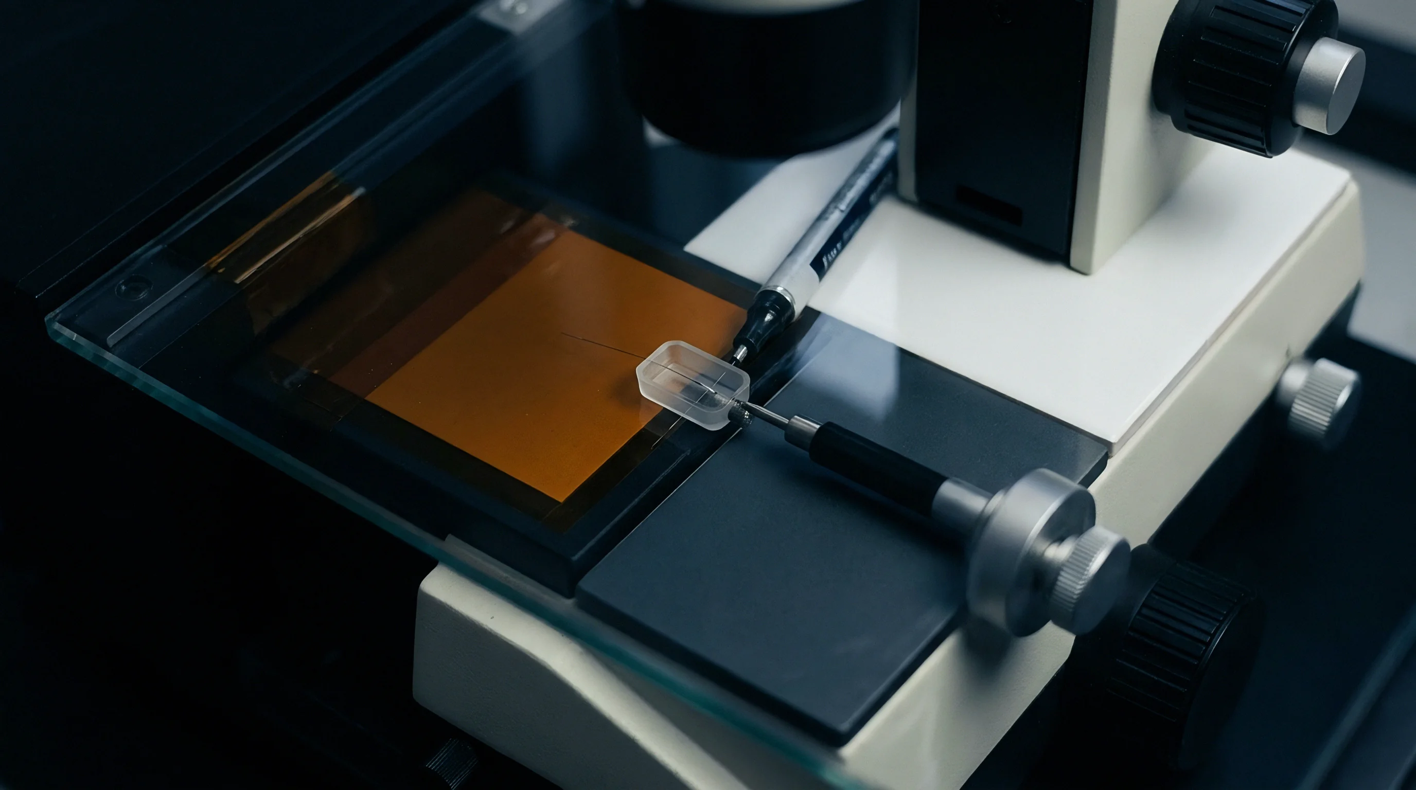
Empirical testing verifies whether microelectromechanical strain isolation features maintain baseline performance under external bending moments and temperature changes. Standard bench-testing protocols that evaluate unmounted components inside thermal chambers fail to capture board-level assembly strain interactions. Complete qualification requires subjecting fully assembled printed circuit board test vehicles to combined mechanical flexure, environmental cycling, and thermal transient testing.
Bench Stress Testing and Reflow Shift Audit
Four-point bending fixtures evaluate sensor zero-g offset stability while applying quantified micro-strain loads to printed circuit board assemblies. A circuit board containing candidate accelerometers mounts inside a calibrated mechanical bending jig. Actuators deflect the board to generate uniform planar strain fields ranging from 100 to 2000 micro-strain.
Continuously reading sensor output during flexure quantifies the strain rejection factor of the decoupling architecture. High-performance decoupled elements limit zero-g bias shift to under 0.05 milligals per micro-strain applied.
Reflow heat induces permanent offset. High thermal profiles encountered during surface-mount technology assembly exceed 260 degrees Celsius. This heat cycle induces plastic deformation within package substrates and cures organic die-attach materials into low-strain baseline states.
Upon cooling, thermal contraction locks residual stresses into the package structure. Tracking zero-g bias before and after solder reflow assembly isolates the permanent stress retention of the packaging system.
- Mount five unpopulated circuit test vehicles containing candidate sensors onto a calibrated four-point bending test rig.
- Apply stepped mechanical deflection up to 2000 micro-strain while recording continuous differential capacitance output.
- Subject assemblies to 250 thermal shock cycles from -40 to +125 degrees Celsius to evaluate die-attach creep and delamination.
- Measure post-reflow zero-g offset drift against baseline pre-assembly calibration dossiers to calculate permanent stress retention.

Sourcing Strategy and Multi-Foundry Risk
Commercial procurement strategy balances high-performance proprietary single-anchor silicon geometries against standardized multi-sourced MEMS foundry processes. Advanced mechanical decoupling architectures, such as suspended sub-frames and central pillar glass-frit bonding, rely on complex multi-wafer processing steps. These specialized processes are typically constrained to single-source MEMS foundries holding specific process patent portfolios.
Relying on sole-source wafer foundries introduces severe supply-chain vulnerability during market allocations or facility disruptions.
| Packaging and Decoupling Tier | Unit Price Target (USD) | Secondary Sourcing Availability | Qualification Lead Time (Weeks) | Target Application Class |
|---|---|---|---|---|
| Standard Overmolded QFN (Direct Die-Attach) | 0.35 – 0.75 | Multiple Foundries | 12 | Consumer Electronics / Wearables |
| Enhanced Overmolded QFN (Silicone + Spring Frame) | 1.20 – 2.50 | Limited Sourcing | 24 | Automotive Stability / Industrial Monitoring |
| Hermetic Ceramic LGA (Central Anchor MEMS) | 4.50 – 12.00 | Sole-Source Process | 36 | Industrial Tilt / Precision Navigation |
| Custom Micro-Cavity TSV (Full Decoupled Frame) | 15.00 – 45.00 | Proprietary Wafer Line | 52 | Defense Guidance / High-Temperature Downhole |
Moisture absorption shifts sensor zero. Standardized surface-mount footprints permit pin-compatible cross-qualification, but internal silicon decoupling designs vary significantly between suppliers. A drop-in alternative part may match electrical pinouts and full-scale range while employing a perimeter-anchored MEMS element.
Substituting a perimeter-anchored part into an assembly optimized for a center-anchored component causes field failures due to increased sensitivity to circuit board warpage. Qualifying alternative sources requires verifying mechanical strain transfer characteristics alongside standard datasheet electrical parameters.
Sole sourcing raises supply exposure. High-volume procurement requires explicit specification of internal silicon anchor topology and package die-attach mechanical properties within purchase contracts. Engineering procurement teams mandate maximum allowable post-reflow zero-g offset shift specifications, forcing suppliers to guarantee structural stress isolation performance across production batches.
It remains unclear whether low-cost molded plastic packages with advanced stress-decoupling springs will ever fully match the long-term zero-g bias stability of hermetic ceramic cavity housings in automotive safety applications.