Silicon Gyroscope Substrate Mechanical Stress Transduction Principles
Packaging and thermal expansion stresses transmit through silicon anchors to shift modal stiffness, generating quadrature errors and uncalibrated bias drift.

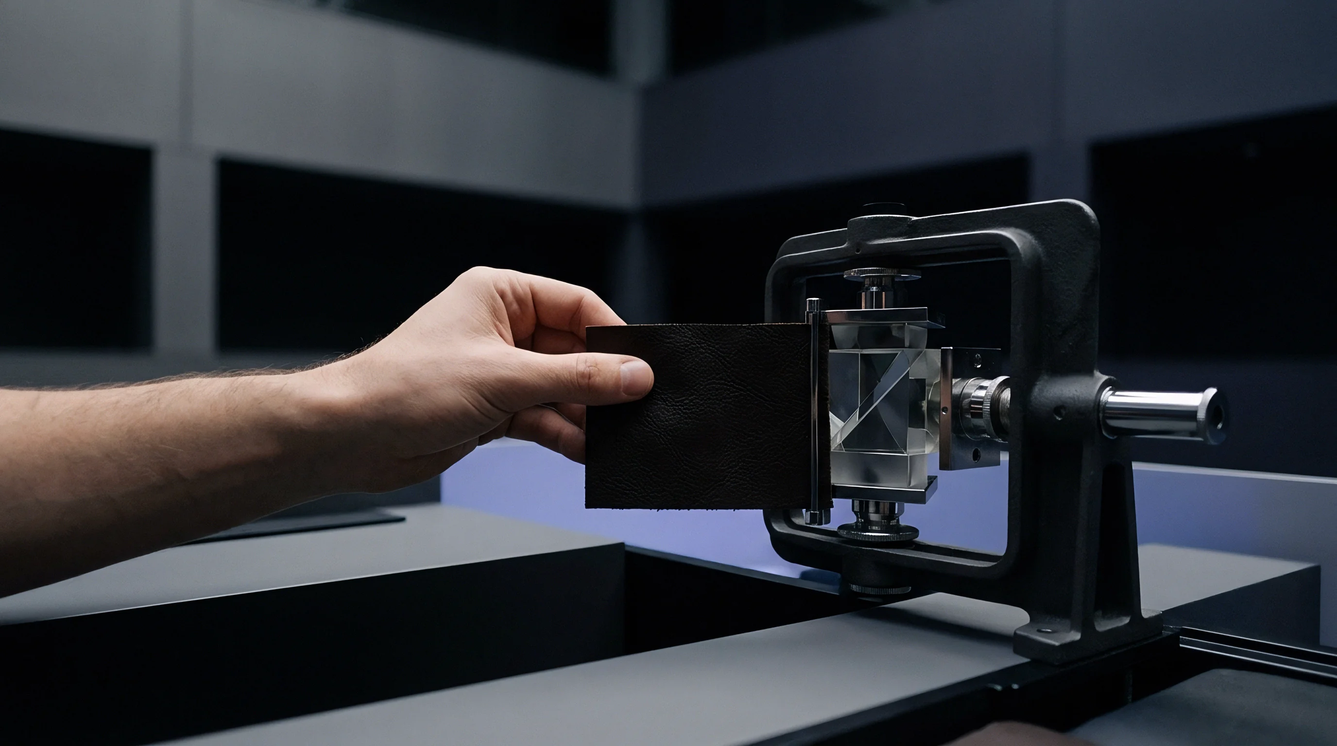
Anchor
Printed circuit board flexure, mold compound contraction, and solder alloy solidification transmit direct mechanical loads through package leadframes into the underlying crystalline silicon die. The silicon substrate acts as a mechanical elastic domain where boundary strains displace structural anchor points, shifting the nominal geometry of suspended micromachined proof masses and folded flexure springs. Rate-sensing transducers operate through the Coriolis acceleration coupling between an intentionally driven primary resonance and an orthogonal secondary sense mode.
Substrate deformations alter the mechanical boundary conditions of these modes, directly modulating resonant frequencies, quality factors, and electrostatic pick-off gaps. A systematic measurement approach treats the silicon die as an active mechanical filter that converts packaging strains into bias drift and scale factor errors.
When external force couples into the package, the die attachment material governs the strain field entering the silicon base. Die-attach adhesives, whether silver-filled epoxies or eutectic gold-silicon alloys, exhibit distinct glass transition temperatures, thermal expansion coefficients, and shear moduli. Mismatch between the coefficient of thermal expansion of the silicon die, typically 2.6 parts per million per Kelvin, and copper leadframes, typically 16.5 parts per million per Kelvin, creates severe residual stress gradients during cooldown from assembly temperatures.
Silicon exhibits severe mechanical stiffness.
| Material Layer | Young Modulus (GPa) | Thermal Expansion (ppm/K) | Poisson Ratio | Stress Relaxation Rate |
|---|---|---|---|---|
| Single-Crystal Silicon (100) | 130 to 169 | 2.6 | 0.064 to 0.28 | Negligible below 500 C |
| Single-Crystal Silicon (111) | 169 to 187 | 2.6 | 0.18 to 0.26 | Negligible below 500 C |
| Leadframe Copper Alloy C7025 | 131 | 16.5 | 0.33 | Elastic at ambient |
| Epoxy Mold Compound (Filled) | 18 to 28 | 8.0 to 14.0 | 0.30 | Viscoelastic above 120 C |
| Die Attach Adhesive (Conductive) | 2.5 to 8.5 | 35 to 55 | 0.38 | Room temperature creep |
| SAC305 Lead-Free Solder | 45 to 52 | 21.5 | 0.36 | Logarithmic creep under load |
Epoxy curing causes volume shrinkage. When resin polymerizes between the die and package pad, shrinkage draws the die corners downward, inducing a spherical or cylindrical warpage profile across the active circuit surface. This die bow displaces surface-micromachined anchor posts relative to one another by displacements ranging from fractions of a nanometer to tens of nanometers.
Suspended folded flexures absorb this relative anchor motion through localized bending moments. The resulting axial loads along suspension flexure beams change the effective spring constant through stress stiffening, modifying both drive and sense fundamental frequencies.
Die warpage shifts resonant frequency splits by 14 Hz per kilopascal of packaging shear stress at 25 degrees Celsius.
Frequency matching governs the sensitivity ceiling in mode-matched gyroscopes, where drive and sense modes share an identical nominal natural frequency. When substrate stress shifts one mode frequency by even 0.05 percent, the mechanical amplification factor of the Coriolis response collapses. In non-mode-matched architectures operating with an intentional frequency split of 1000 Hz, an anchor displacement altering the split by 20 Hz produces an uncalibrated scale factor shift exceeding two percent.
Transduction physics links packaging boundary displacements to open-loop rate errors that downstream digital compensation algorithms struggle to eliminate.
The transmission path continues through the capacitive comb fingers and parallel-plate sense electrodes. Substrate strain warps the stator finger anchors while leaving rotor fingers positioned by suspension beams, altering nominal capacitive gaps unequally across balanced differential pairs. Gap variations scale inversely with electrostatic force and pick-off charge, introducing zero-rate bias offsets that track mechanical board strain rather than angular velocity.
Solder assembly schedules and chassis screw torque values therefore enter the sensing equation as primary operational variables.


Anisotropy
Single-crystal silicon lacks isotropic mechanical behavior, displaying directional dependence governed by fourth-rank elasticity tensors. The wafer growth orientation fixes the directional elastic moduli along crystallographic axes. In standard (100) silicon wafers, Young modulus varies from 130 GPa along the <100> directions to 169 GPa along the <110> directions, while shear modulus drops from 79.6 GPa to 50.9 GPa across the same angular sweep.
Planar biaxial stresses imposed by symmetric packaging geometries yield asymmetric internal strain fields within the suspension flexures due to this directional stiffness variation.
Mechanical compliance differences induce planar skewing. Suspended ring resonators or tuning fork tethers fabricated along varying crystallographic angles deflect asymmetrically under uniform package compression. A perfectly circular ring resonator distorts into an ellipse when uniform compressive stress excites the anisotropic compliance tensor of the underlying silicon die, shifting the orientation of vibration nodes away from designed capacitive pick-off electrodes.
Shear stress rotates principal axes.
Compliant sub-mounts trade mechanical shock survivability for thermal bias stability.

Where Does Piezoresistive Coupling Corrupt Differential Detection?
Electrical conductivity in doped single-crystal silicon shifts linearly with mechanical stress tensors via piezoresistive coupling coefficients. When polysilicon or single-crystal silicon flexures experience localized tensile and compressive strains during proof mass displacement, residual package stresses modify the background resistivity of conducting routing traces. Substrate stress creates asymmetrical resistance shifts in balanced push-pull capacitive readout topologies, converting common-mode thermal expansions into differential electrical offsets.
The piezoresistive tensor components pi-11, pi-12, and pi-44 in p-type silicon reach magnitudes up to 138 times ten to the negative eleventh square meters per Newton, producing millivolt-level bias offsets across transimpedance amplifier inputs when mounting stress is present.
Silicon piezoresistance links mechanical packaging distortion directly to electronic sensor drift through four primary mechanisms:
- Bulk resistivity modulation shifts parasitic trace impedances across differential sensing channels, breaking charge amplifier bridge balance under board torque.
- Piezojunction leakage shifts alter diode leakage currents within electrostatic discharge protection structures, introducing microvolt offset voltages into high-impedance sense nodes.
- Capacitive gap modulation alters stator finger pitch through anchor pitch variations, unbalancing differential sense pairs.
- Thermal piezoresistive interaction creates second-order temperature drift coefficients that bypass polynomial calibration models implemented in application-specific integrated circuits.
Piezoresistive coupling demands exact orientation of critical mechanical suspensions along crystallographic axes that minimize coupling coefficients. Designers orient critical flexures along the <100> direction in p-type substrates to suppress the large shear piezoresistance coefficient pi-44. Wafers with (111) surface orientation provide isotropic planar Young modulus values of 169 GPa, eliminating planar directional stiffness variations at the expense of higher material raw costs and specialized chemical etching characteristics during deep reactive ion etching processes.
Symmetric geometric arrangements fail to cancel substrate stress when crystal axes diverge from mechanical symmetry vectors. An engineer who aligns gyroscope suspension tethers without tracking the crystallographic notch location on the raw silicon wafer allows directional packaging strains to bypass structural cancellation paths. Unchecked crystallographic misalignment degrades long-term bias stability.

Quadrature
Mechanical cross-coupling between drive and sense axes generates a spurious acceleration signal ninety degrees out of phase with the actual Coriolis velocity response. Under ideal manufacturing conditions, the drive motion of a proof mass stays strictly confined to its actuation plane. Substrate stress transmitted through mounting anchors alters this orthogonality by introducing out-of-plane tilt or in-plane skewing across suspension anchor posts.
Comb fingers displace laterally.
When substrate warpage induces asymmetric compliance across folded support beams, proof mass drive actuation couples parasitic forces into the sense axis. A drive displacement of 10 micrometers requires only a 0.01 degree tilt in the suspension spring alignment to generate an apparent sense displacement of 1.74 nanometers. Given that typical full-scale Coriolis displacements span sub-picometer dimensions, mechanical quadrature signals frequently exceed the actual rate signal by three to four orders of magnitude at the pick-off electrodes.
Drive energy leaks into sense.
| Stress Mode | Primary Physical Mechanism | Output Error Signature | Mitigation Strategy |
|---|---|---|---|
| Biaxial Planar Compression | Buckling stress in suspension beams; frequency stiffening | Scale factor drift; mode split widening | Single center-anchor mounting; stress relief loops |
| Out-of-Plane Bending (Die Bow) | Anchor post angular tilt; comb overlap area variation | Quadrature error surge; charge amplifier saturation | Thick silicon cap bonding; nested gimbal frames |
| In-Plane Die Shear Stress | Anisotropic spring constant modification; axis skewing | Zero-rate output bias shift; cross-axis sensitivity | Crystallographic axis alignment; balanced push-pull combs |
| Localized Mounting Point Torque | Asymmetric capacitive stator displacement | Thermal hysteresis; long-term bias instability | Compliant silicone die attach; decoupled package islands |
Demodulation architectures extract angular rate by multiplying the amplified sense signal with a phase-synchronized drive reference signal, rejecting the orthogonal quadrature component. Phase errors within the demodulation clock instantly compromise this separation. If the reference clock drifts by a phase margin of 0.1 degree due to substrate strain shifting drive tank filter parameters, a quadrature signal measuring 1000 degrees per second leaks into the in-phase channel, producing an uncorrectable zero-rate bias shift of 1.74 degrees per second.
Phase margins degrade under load.
Differential sense architectures suppress common-mode expansion while amplifying packaging twist.
Capacitance changes invert rapidly. High quadrature voltages generated across sense pick-off fingers reduce the dynamic range available for genuine rate measurement within front-end continuous-time charge amplifiers. Severe substrate warpage can drive input operational amplifiers into hard rail saturation, causing total telemetry loss during board soldering operations or shock events.
Electronic quadrature compensation loops mitigate this risk by applying static DC voltages to dedicated compensation electrodes, creating electrostatic negative stiffness that pulls suspension flexures back toward orthogonality. Electrostatic trim requires active DAC headroom and increases total application-specific integrated circuit power consumption.
Failure to constrain mechanical quadrature generation at the substrate anchor boundary forces the signal chain to manage massive dynamic range spreads, driving amplifier noise floors upward and consuming sensor dynamic range budgets.


Isolation
Mechanical decoupling structures positioned between the silicon substrate boundary and active transducer suspensions intercept packaging strains before they reach resonant flexures. Advanced micromachining incorporates deep silicon trenches, suspended sub-frames, and localized anchor architectures to attenuate stress propagation. A single central anchor topology connects the entire active proof mass suspension to the substrate through a solitary silicon pillar positioned at the exact geometric and crystallographic center of the die.
Center pedestals minimize moment arms.
Planar package expansions and contractions expand radially outward from a central pedestal without applying relative displacement across paired suspension anchors. Differential thermal expansion between die and package generates minimal shear stress across an anchor footprint confined to a radius under 200 micrometers. Peripheral multipoint anchors, conversely, span die distances of three to five millimeters, accumulating hundreds of nanometers of relative displacement during thermal excursions.
Resonator modes decouple across symmetry.

What Drives Bias Instability across Solder Reflow Profiles?
Peak temperatures during lead-free solder reflow reach 260 degrees Celsius, melting SAC305 alloy paste and softening package mold compounds above their glass transition points. As assemblies cool past solidus temperatures, package resins lock residual stress fields into the leadframe and silicon backing. Subsequent ambient storage exposes these polymeric and metallic bonds to room-temperature viscoelastic creep, altering the stress profile applied to substrate anchors over hundreds of operating hours.
Solder joints creep over time.
Engineering teams mitigate post-reflow mechanical instability by deploying multiple structural decoupling stages throughout the packaging stack:
- Substrate stress relief trenches etched through the active device layer isolate anchor attachment zones from peripheral die cutting edges where wafer dicing induces micro-fractures.
- Nested compliant gimbal frames encircle the proof mass, absorbing in-plane die warpage through high-aspect-ratio folded flexures before shear loads reach primary suspension posts.
- Low-modulus die attach silicones with Young moduli below 10 MPa replace stiff epoxy adhesives, absorbing board flexure strains via large elastic shear deflections.
- Thick silicon capping wafers bonded via glass frit or direct silicon fusion create rigid micro-cavity shells, resisting package compression forces through high structural moment of inertia.
Silicon capping wafers perform a dual role: sealing resonant structures within ultra-high vacuum environments below 0.01 millibar while stiffening the active die sandwich against out-of-plane bending. Anodic bonding of Borofloat glass caps introduces thermal expansion mismatches that generate permanent parabolic residual stress profiles across silicon resonators. Direct silicon-to-silicon fusion bonding eliminates this interfacial thermal mismatch, maintaining planar stress uniformity through subsequent package overmolding steps.
| Isolation Architecture | Stress Attenuation Factor | Die Area Overhead | Shock Fragility Ceiling | Thermal Hysteresis (deg/hr) |
|---|---|---|---|---|
| Direct Multipoint Peripheral Anchor | 0 dB (Reference) | 0 % | > 20,000 g | 15.0 to 45.0 |
| Single Central Post Anchor | 22 to 28 dB | 12 to 18 % | 5,000 to 8,000 g | 1.5 to 4.0 |
| Nested Outer De-Coupling Ring Frame | 18 to 24 dB | 20 to 30 % | 10,000 to 12,000 g | 2.0 to 6.0 |
| Folded Anchor Tether Relief Trenches | 14 to 18 dB | 8 to 14 % | 12,000 to 15,000 g | 4.5 to 9.0 |
| Dual-Cavity Symmetric Cap Sandwich | 26 to 34 dB | 40 to 60 % | 3,000 to 6,000 g | 0.3 to 1.2 |
Suppliers frequently assert that internal digital temperature compensation look-up tables fully eliminate the operational consequences of package stress without requiring complex die-level isolation frames. Thermal expansion mismatches break alignment. Board-level bending strains applied through chassis torquing operate independently of temperature, generating bias shifts that completely elude look-up tables calibrated solely against on-chip temperature sensors.

Screening
Incoming inspection procedures and production screening protocols must separate genuine angular velocity response from mounting stress sensitivity before sensors enter final system integration. Accelerating environmental stress screening forces packaging assemblies through thermal shock, high-temperature storage, and random vibration regimes. Thermal cycling degrades bias repeatability.
Packaging stresses that fail to relax elastically manifest as irreversible zero-rate bias shifts across thermal transition baselines.
Wafer-level testing measures baseline resonance frequencies and quality factors before dicing, providing an unstressed reference state for every die. Comparing these wafer-level baselines against post-packaging final test data reveals the exact frequency shift induced by packaging stress. Dies displaying modal frequency shifts exceeding 50 parts per million indicate defective die attach coverage, voiding in adhesive layers, or excessive mold compound contraction.
Leadframe alloys impose high stress.
IEC 60721-3-7 Class 7M3 specifies random vibration spectral densities that induce dynamic substrate strains exceeding 120 microstrain along unisolated die edges.
Board-level reliability testing demands continuous monitoring of sensor output while test boards experience four-point mechanical bend testing under controlled displacement limits. Solder pad layout geometries dictate the distribution of trace-transmitted strains into plastic leadless chip carrier (LCC) and quad-flat no-leads (QFN) packages. Placing gyroscopes near circuit board mounting screw holes or heavy inductors subjects the substrate to sustained strain fields exceeding 200 microstrain, shifting factory-trimmed bias points outside specification bounds.
Drift budgets vanish immediately.
Procurement contracts incorporate specific compliance clauses based on standard IPC-9701 performance conditions. The purchase specification enforces that component zero-rate output drift must remain within 0.5 degrees per second following five consecutive passes through a lead-free solder reflow thermal profile reaching 260 degrees Celsius peak temperature. A contract clause governing board-level mechanical strain limits supplier liability when board layout engineers place components within restricted high-strain zones adjacent to circuit board mounting points.