Thermal Margin
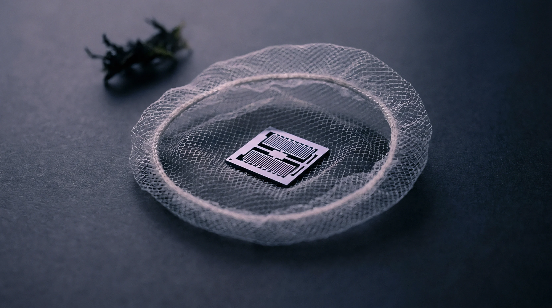
A mechanical decoupling layer positioned directly beneath a semiconductor die to absorb thermo mechanical shear strains generated by mismatch in coefficients of thermal expansion between dissimilar packaging substrates. Package stress isolation restricts residual warpage during cooling phases of the reflow soldering cycle by introducing an elastomeric boundary that cushions differential contraction vectors. Residual stresses migrate into the intermediate compliant sublayer rather than transmitting directly into brittle silicon interconnects or intermetallic compound layers.
The protection window remains effective up to the glass transition temperature of the elastomer, beyond which modulus degradation permits direct force transfer across the bondline.
Boundary Compliance
Material selection relies upon balancing shear modulus against permanent creep deformation under sustained elevated temperature storage. Package stress isolation depends upon viscoelastic damping characteristics that dissipate mechanical energy through internal molecular friction instead of elastic rebound. Manufacturers set baseline compliance thresholds using dynamic mechanical analysis to measure loss tangent parameters across expected operating temperature sweeps.
Environmental aging degrades this damping capacity through moisture ingress and plasticizer migration, which gradually stiffens the interface and raises transmitted shear forces.
Interconnect Protection
Solder joint fatigue life extends significantly when microelectronic assemblies incorporate strain relief barriers that interrupt crack propagation pathways. Package stress isolation prevents cyclic thermal excursions from shearing microscopic copper pillars connecting the substrate to the motherboard. Finite element modeling calculates plastic work accumulation within each joint array by simulating thermal shock loading profiles derived from military and automotive standards.
Field failures concentrate at the perimeter of large form factor ball grid arrays where differential displacement reaches maximum amplitude.
Fabrication Tolerance
Assembly verification requires dimensional inspection of the elastomer thickness profile using optical coordinate measuring systems before encapsulation steps occur. Package stress isolation tolerances are governed by semiconductor packaging specifications that dictate strict planarity limits across the entire substrate footprint. Deviations in dispense volume create localized thickness variations that alter thermal resistance paths and induce tilting moments during die attach curing.
Post lamination metrology verifies that the decoupling layer maintains uniform thickness across all active circuitry zones to prevent asymmetric mechanical loading during subsequent overmolding processes.