High Temperature Interfacial Oxygen Diffusion and Void Nucleation Kinetics in Multilayer Sensor Passivations
High temperature oxygen diffusion across sensor passivations triggers interfacial void nucleation, driving sensor zero-point drift past operational limits.


Transport
Anion migration through solid dielectric barriers accelerates sharply when sensor operating environments exceed 500 °C. Platinum thin-film resistors, zirconia exhaust probes, and silicon carbide pressure transducers rely on thin dielectric caps to isolate conductive metallization layers from reactive ambient gases. In oxidizing environments at high temperatures, oxygen traverses the passivation layer along grain boundaries, structural micro-cracks, and lattice vacancies. This ingress alters the underlying electrode chemistry, modifies interface work functions, and produces monotonic baseline drift in precision transducer circuits, with oxygen flux accelerating further above 600 °C.
Quantifying mass transfer through multilayer passivations requires separating bulk lattice diffusion from grain boundary transport. In polycrystalline oxide layers deposited by physical vapor deposition, grain boundary diffusion coefficients exceed lattice coefficients by three to five orders of magnitude. The effective diffusion coefficient follows a standard Arrhenius relationship where the pre-exponential factor and activation energy depend strictly on film microstructure and deposition stoichiometry.
Amorphous films deposited by atomic layer deposition eliminate high-angle grain boundaries entirely, raising the effective activation energy for oxygen transport from 1.2 eV in sputtered polycrystalline films to over 2.1 eV in dense amorphous aluminum oxide.
Oxygen anion diffusion in sputtered alumina reaches 2.4 x 10^-17 cm^2/s at 750 °C under ambient atmospheric pressure.
Chemical potential gradients across the passivation boundary establish the primary driving force for anion motion. In high-temperature gas sensors, the oxygen partial pressure differential between the process gas and the buried metallic thin film generates an electrochemical drift force that compounds standard concentration-driven diffusion. When unpassivated or weakly passivated platinum sensing elements react with ingressed oxygen, transient sub-surface platinum oxide phases form, altering the effective cross-sectional area of the resistive trace and changing the nominal resistance value.

Thin Film Oxygen Permeation Rates
Dielectric layers exhibit distinct permeation regimes governed by their deposition density, thermal history, and defect density. Sputtered silicon dioxide films frequently contain columnar morphologies that provide direct paths for diatomic and ionic oxygen species. By contrast, stoichiometric hafnia, zirconia, and alumina nanolaminates form tortuous diffusion paths when deposited in alternating layers with individual thicknesses below ten nanometers.
| Material Layer | Deposition Process | Activation Energy (eV) | Diffusion Coefficient (cm²/s) | Transport Mechanism |
|---|---|---|---|---|
| Silicon Dioxide (SiO₂) | Plasma Enhanced CVD | 1.15 ± 0.08 | 4.2 x 10^-15 | Columnar boundary migration |
| Polycrystalline Al₂O₃ | DC Magnetron Sputtering | 1.45 ± 0.10 | 8.6 x 10^-16 | Grain boundary transport |
| Amorphous Al₂O₃ | Atomic Layer Deposition | 2.10 ± 0.12 | 3.1 x 10^-18 | Bulk interstitial vacancy hopping |
| HfO₂ / Al₂O₃ Nanolaminate | Atomic Layer Deposition | 2.35 ± 0.15 | 7.4 x 10^-19 | Interface trapping and tortuous path |
| Silicon Nitride (Si₃N₄) | Low Pressure CVD | 1.80 ± 0.11 | 1.2 x 10^-16 | Defect-assisted interstitial drift |
Calculations for annual oxygen ingress through a 100-nanometer barrier layer demonstrate the operational sensitivity of sensor passivations. A sensor operating continuously at 700 °C beneath an amorphous nanolaminate layer experiences an oxygen mass transfer rate of less than 0.02 nanograms per square millimeter per year. Under an identical thermal load, a standard sputtered silicon dioxide layer permits over 110 nanograms of oxygen transfer per square millimeter annually, triggering catastrophic oxidation of underlying adhesion promoters like titanium or tantalum within three hundred operating hours.

Defect Mediated Anion Drift across Bilayers
Point defects within the oxide lattice dictate local transfer rates when external electrical fields exist across the sensor structure. Oxygen vacancies act as positively charged transport vehicles in non-stoichiometric metal oxide barriers. During operation under bias, such as in capacitive pressure sensors or resistive temperature detectors, applied electric fields superimpose an electrostatic drift velocity onto the random thermal diffusion of vacancies.
While standard high-temperature burn-in treatments are intended to stabilize these thin-film interfaces prior to delivery, unverified thermal aging merely advances the depletion zone without halting ongoing oxygen transmission.


Pore
Cavity creation along material boundaries represents the primary structural degradation mode in multilayer sensor passivations operating above 500 °C. When oxygen anions diffuse through the passivation cap and react with underlying metals or adhesion layers, unequal atomic flux rates generate local supersaturations of vacancies. This phenomenon, rooted in the classic Kirkendall effect, causes vacancies to coalesce into discrete sub-micrometer cavities along the metal-dielectric interface.
Local stress fields accelerate vacancy aggregation. Thermal expansion mismatches between the passivation ceramic (such as alumina with a thermal expansion coefficient around 8 x 10^-6 /K) and the underlying sensing metal (such as platinum with a coefficient near 9 x 10^-6 /K, or gold at 14 x 10^-6 /K) produce substantial interfacial shear stresses during thermal cycling. These shear stresses create triaxial tensile stress zones near interface step-edges, micro-ridges, and contact vias.
Vacancies preferentially migrate toward regions of elevated hydrostatic tension, lowering the critical thermodynamic barrier required for stable cavity nucleation.
Dense amorphous dielectric stacks suppress interfacial vacancy clustering by eliminating continuous grain boundary paths.
As interfacial voids expand and merge, mechanical delamination occurs, decoupling the sensor trace from its substrate and degrading thermal conduction paths. In thin-film platinum temperature sensors, interfacial separation isolates sections of the resistive trace from the substrate heat sink, causing local Joule overheating and loss of ohmic contact during measurement excitation. The resulting localized hot spots accelerate regional chemical reactions, leading to abrupt positive resistance jumps and terminal open-circuit failures.
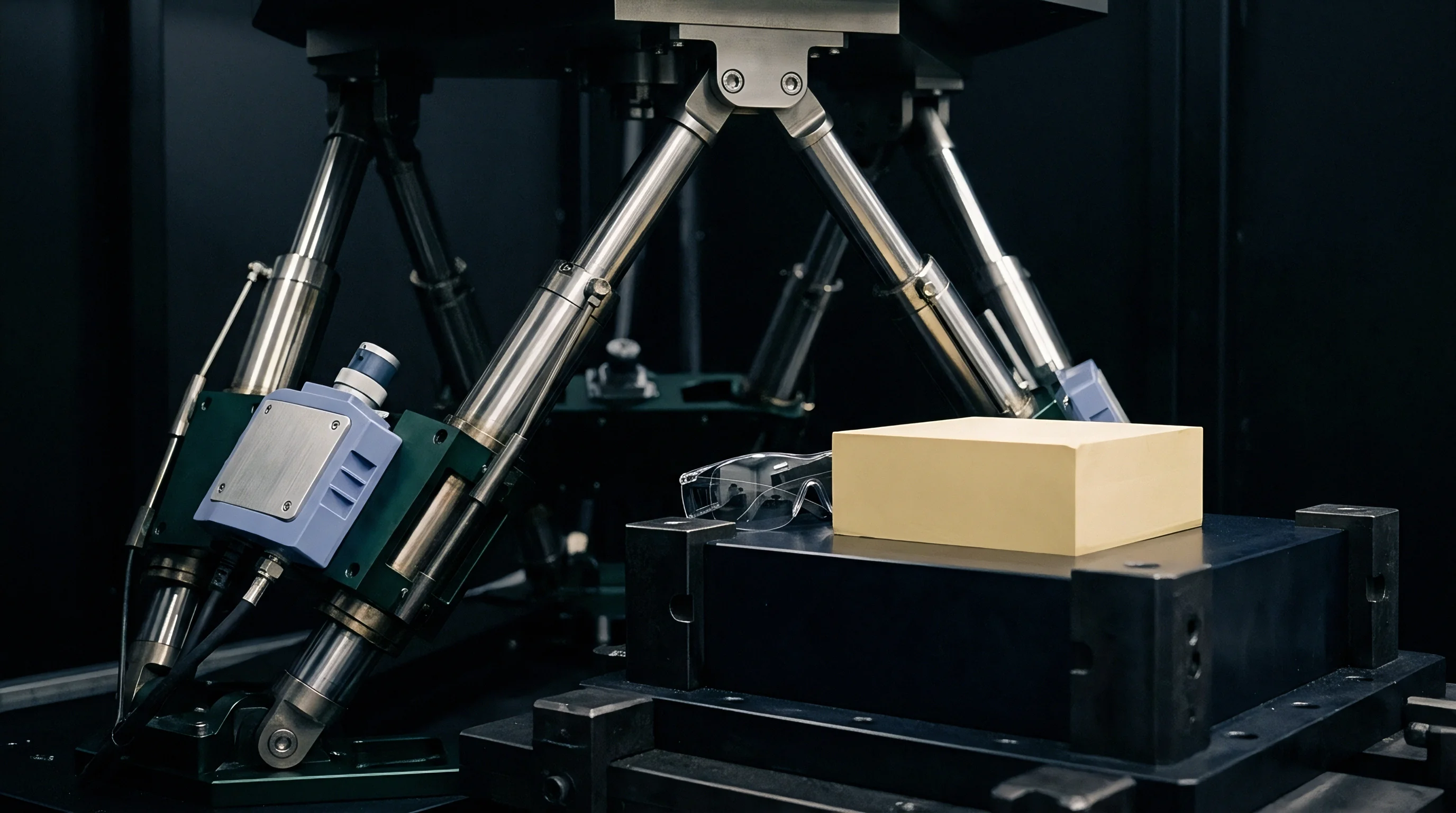
Vacancy Condensation at Metal Ceramic Boundaries
Thermodynamic models define the critical radius for a stable void nucleus through the balance between volumetric strain energy relief and surface energy penalties. At high temperatures, the steady-state vacancy concentration exceeds equilibrium levels because of continuous chemical reactions at the interface. The critical radius decreases as vacancy supersaturation climbs, allowing cavities as small as two nanometers to become thermodynamically viable and grow spontaneously.
The progression of interfacial damage moves through distinct morphological stages that correlate directly with transducer signal degradation:
- Initial Vacancy Clustering occurs within the first atomic layers of the metal-passivation boundary, producing sub-three-nanometer vacancy aggregates that remain undetectable by conventional acoustic microscopy while altering interface contact resistance by fractions of a percent.
- Cavity Coalescence proceeds along grain boundary intersections where localized tensile stress concentrates vacancy flux, forming planar void networks that cover between five and twenty percent of the active interface area.
- Interfacial Delamination develops when interconnected micro-voids separate the dielectric film from the underlying metallization, reducing mechanical peel strength below three megapascals and inducing significant thermal isolation.
- Blistering and Rupture takes place as trapped gaseous species or extreme compressive thermal stresses cause the unbonded passivation membrane to buckle upward, fracturing the dielectric cap and exposing raw metallization to the atmosphere.
As capacitance drops across these failed zones, the practical result on the test bench appears as unrecoverable zero-point drift, widening calibration hysteresis, and sudden step-function changes in sensor output during thermal transients.
| Passivation Architecture | Metallization Layer | Mean Void Nucleation Time (h) | Area Fraction Voided at 1000h (%) | Interfacial Shear Strength (MPa) |
|---|---|---|---|---|
| SiO₂ (200 nm) / Ti (10 nm) | Pt (150 nm) | 45 ± 6 | 38.2 ± 4.1 | 12 ± 2 |
| Al₂O₃ (100 nm) / Ta (15 nm) | Pt (150 nm) | 180 ± 15 | 14.6 ± 1.8 | 28 ± 4 |
| Al₂O₃ (50 nm) / HfO₂ (50 nm) | Pt (150 nm) | 620 ± 40 | 3.1 ± 0.5 | 65 ± 5 |
| Si₃N₄ (150 nm) / TiW (20 nm) | Au (200 nm) | 85 ± 10 | 29.4 ± 3.2 | 18 ± 3 |
| Al₂O₃/ZrO₂ Nanolaminate (120 nm) | Pt (150 nm) | 1150 ± 75 | 0.8 ± 0.2 | 82 ± 6 |

Kirkendall Cavitation Dynamics during Thermal Cycling
Thermal excursions compound vacancy supersaturation by cycling the sign and magnitude of interfacial shear stress. During cooling phases, differential thermal contraction generates tensile stresses in metallization films deposited at high substrate temperatures, driving vacancy diffusion along the metal grain boundaries toward the passivation interface. During subsequent heating cycles, compressive stresses alter local chemical potentials, redirecting vacancy condensation patterns.
Whether atomic mobility along nanolaminate sub-interfaces can be engineered to absorb excess vacancies without nucleating critical cavities remains an open physical question.


Barrier
Passivation architectures engineered for service beyond 600 °C utilize multiple alternating layers of distinct dielectric oxides to suppress both ionic transport and mechanical void formation. Monolithic single-layer passivations fail prematurely because grain boundaries extend continuously through the entire film thickness, providing direct expressways for ambient species. Multilayer structures disrupt these continuous pathways by introducing sharp crystallographic and chemical transitions at every sub-layer interface, where grain boundaries otherwise dominate mass transport.
Atomic layer deposition enables the synthesis of nanolaminates combining high bandgap materials with high dielectric constant oxides. In an alternating aluminum oxide and hafnium oxide nanolaminate, each layer transition interrupts grain growth, forcing the individual films to retain either an amorphous phase or a fine nanocrystalline structure. The dense interfaces between dissimilar oxides create electrostatic potential barriers that increase the effective activation energy required for oxygen anion migration.
Interfacial cavities decrease effective active contact area and raise local current densities across sensing electrodes.
Adhesion promotion layers beneath the primary dielectric stack govern the mechanical integrity of the entire assembly. Conventional titanium and chromium adhesion layers oxidize rapidly at temperatures above 400 °C, drawing oxygen through the dielectric cap and generating expanding oxide volumes that crack the overlying passivation. Replacing reactive base metals with refractory metal oxides, conducting nitrides such as titanium aluminum nitride, or ultra-thin noble metal alloys preserves interface bonding without feeding vacancy condensation mechanisms.

Stoichiometric Alumina and Hafnia Dielectric Stacks
Thin film stacks combining amorphous alumina with crystalline hafnia leverage complementary physical attributes. Amorphous alumina provides hermetic sealing against gaseous diffusion, while hafnia imparts thermodynamic stability and resistance to reduction in hydrogen-rich process streams. Controlling the sub-layer thickness to values below five nanometers prevents hafnia from transitioning into its monoclinic phase, preserving an amorphous or cubic nanocrystalline structure with superior fracture toughness.
Selecting materials for high-temperature sensor passivations involves verifying four physical criteria:
- Thermodynamic Free Energy of Oxide Formation must exceed negative eight hundred kilojoules per mole of oxygen to prevent reduction by ambient reducing gases or adjacent metallic traces.
- Thermal Expansion Matching requires the composite stack thermal expansion coefficient to fall within 1.5 x 10^-6 /K of the sensor substrate to limit thermal shear stresses during process cycles.
- Crystallization Temperature Threshold must remain at least one hundred degrees Celsius above the maximum operational temperature to prevent post-deployment grain boundary network formation.
- Dielectric Breakdown Field Strength must remain above five megavolts per centimeter at peak operating temperature to prevent leakage currents from distorting microvolt-level sensor bridge outputs.
These material constraints dictate that passive caps undergo qualification testing at temperature extremes exceeding normal process conditions by at least fifty degrees Celsius.

Interfacial Trapping and Grain Boundary Passivation
Doping dielectric interfaces with rare-earth cations, such as yttrium or lanthanum, provides localized chemical traps for oxygen vacancies. The large ionic radius of yttrium segregates to the interface boundaries, distorting the local coordination environment and immobilizing vacancies that would otherwise participate in diffusion and coalescence. This localized doping raises the activation energy for interfacial void nucleation by more than 0.6 eV.
Dense amorphous nanolaminates without continuous vertical grain boundaries consistently outlast single-layer polycrystalline dielectrics in high-temperature environments.


Assay
Physical verification of diffusion barrier performance and void kinetics requires high-resolution depth-profiling techniques paired with in-situ electrical tracking. Standard room-temperature bench testing fails to reveal developing vacancy networks, as interfacial voids only alter macroscopic sensor impedance once delamination or significant oxidation has already occurred. Systematic qualification combines isotopic oxygen tracer exposure, secondary ion mass spectrometry depth profiling, and continuous high-temperature potentiostatic resistance tracking.
Secondary ion mass spectrometry utilizing the oxygen-18 isotope provides unambiguous quantification of oxygen transport through dielectric stacks. Test samples undergo annealing in an enriched oxygen-18 atmosphere at target operational temperatures for durations ranging from one hundred to one thousand hours. Depth profiling through the passivation stack tracks the exact penetration profile of the isotope, allowing calculation of the true diffusion coefficient without confounding data from pre-existing oxygen in the oxide lattice.
IEC 60068-2-2 dry heat testing at 800 °C shifts unpassivated thin-film resistance beyond specified Class A tolerances within forty-eight hours.
Cross-sectional transmission electron microscopy combined with energy-dispersive X-ray spectroscopy confirms whether oxygen penetration has reached the metallic sensor interface. High-angle annular dark-field imaging identifies sub-nanometer void clusters long before they merge into macroscopic delamination planes, providing an early warning metric for long-term calibration stability.

Secondary Ion Mass Spectrometry Depth Profiles
Analyzing depth profiles requires careful extraction of background noise and instrument artifacts. Sputter rate calibration using optical profilometry on the crater floor ensures depth accuracy within two nanometers across a two-hundred-nanometer stack. When oxygen-18 concentrations at the metal interface exceed 0.1 atomic percent, the underlying metallization faces imminent oxidation and resistance drift.
Executing an incoming batch qualification for thin-film passivations follows a rigorous analytical sequence:
- Baseline Spectral Reflectometry measures thickness and refractive index across a nine-point wafer matrix to verify dielectric layer uniformity within a three percent tolerance window.
- Isotopic Tracer Thermal Annealing exposes sample coupons to a 95 percent oxygen-18 environment at 750 °C for two hundred hours inside an ultra-clean quartz tube furnace.
- Dynamic SIMS Sputter Profiling records secondary ion counts for oxygen-18, oxygen-16, aluminum, hafnium, and underlying platinum down to a depth fifty nanometers below the active interface.
- Automated Void Detection Analysis utilizes high-resolution transmission electron micrographs to quantify cavity density per unit interface length and calculate total voided area fraction.
Because pinholes short the active junction, skipping any phase of this verification chain exposes the deployment fleet to unquantified sensor drift and unpredictable early-life field failures.
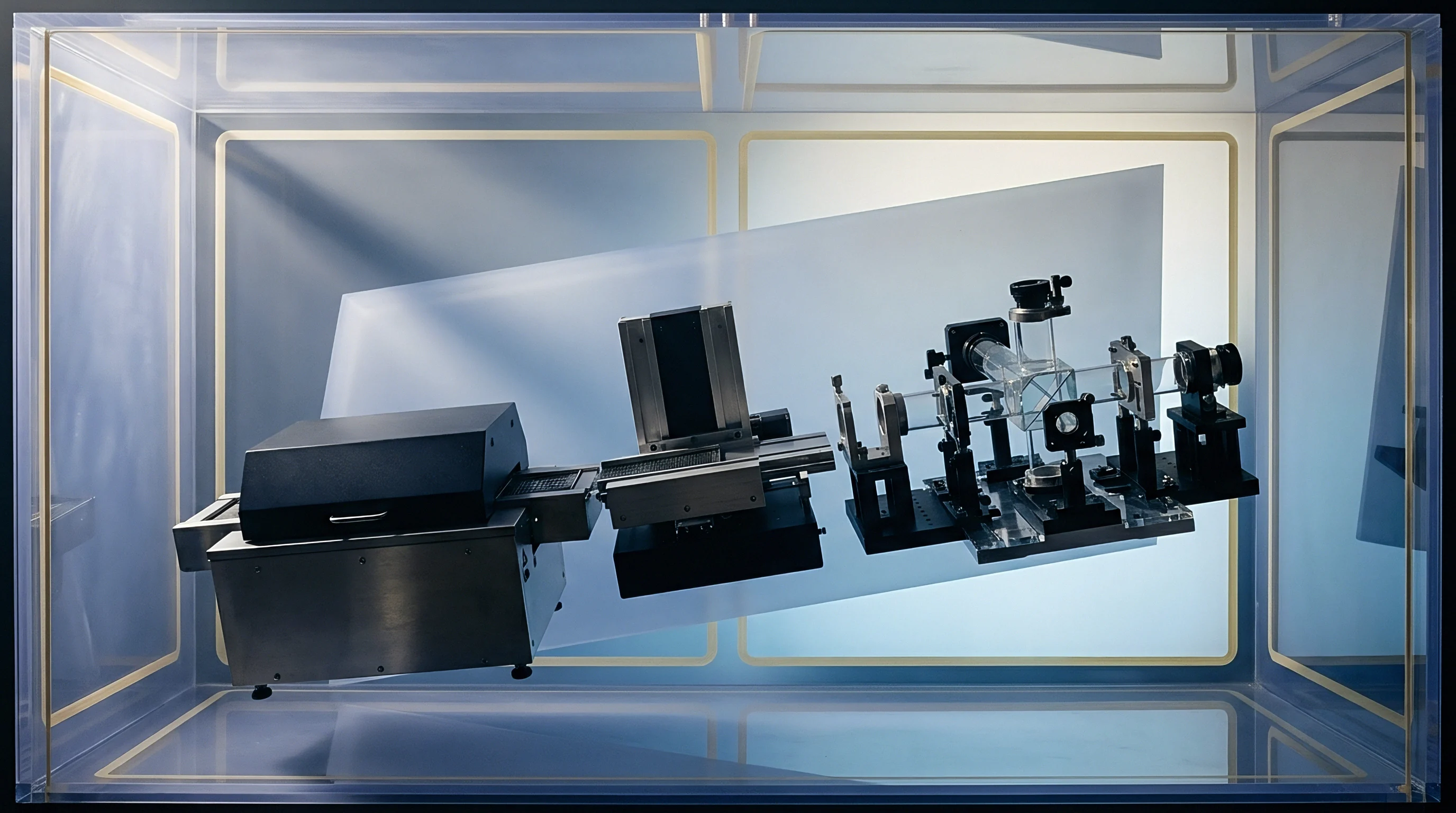
Potentiostatic Sensor Drift Tracking across Temperature
Continuous electrical measurement during isothermal soaking reveals the direct functional manifestation of interfacial degradation. A constant direct current bias applied across a thin-film resistance temperature detector placed in an 750 °C dry air chamber produces a baseline resistance drift curve. In uncompromised passivations, the drift curve exhibits a sub-linear, diffusion-limited profile.
The sudden onset of linear or exponential drift indicates passivation cracking or rapid void coalescence.
Contractual specifications referencing IEC 60751 Class AA stability criteria designate a maximum permissible resistance drift of 0.04 percent after one thousand hours at peak rated temperature, which automatically disqualifies any sensor lot showing interfacial void area fractions greater than two percent during accelerated physical testing.


Warranty
Sensor drift resulting from interfacial voiding and oxygen diffusion translates directly into measurement uncertainty, invalidating calibration certificates and shortening permissible re-calibration intervals. When industrial processes rely on high-temperature sensors for safety shutdowns, emissions monitoring, or tight thermal regulation, unverified drift increases financial risk and opens significant liability exposure unless drift figures are supported by verified test durations.
A precision platinum thin-film sensor specified to maintain a Class A tolerance of ±0.35 °C at 500 °C can drift beyond its operational envelope within six months if interfacial voids consume more than five percent of the electrode contact perimeter. The loss of cross-sectional metal area increases base trace resistance, mimicking a positive temperature shift. For a continuous chemical furnace operating at 600 °C, an undetected +1.5 °C sensor drift can alter product yields, degrade catalyst beds, and violate environmental discharge permits.
Field failures mount after one year. Re-calibration expenses rapidly surpass the original purchase price of the sensor hardware when devices must be extracted from hazardous, pressurized, or ultra-clean process chambers. Specifying a premium multilayer nanolaminate passivation adds approximately fifteen to twenty-five percent to the base procurement cost per unit, yet it eliminates mid-cycle sensor extraction and extends calibration validity from six months to thirty-six months in continuous service.

Calibration Interval Extension and Yield Retention
Calculating the true landed cost of measurement accuracy requires modeling total lifecycle expenses across the sensor operating lifetime. Sourcing managers frequently evaluate sensor options based on initial unit purchase price while neglecting the compounded labor, process downtime, and laboratory calibration fees required to support drift-prone hardware.
| Cost Component | Single-Layer Sputtered SiO₂ | Bilayer Al₂O₃ / Ta Cap | ALD Al₂O₃ / HfO₂ Nanolaminate |
|---|---|---|---|
| Initial Unit Procurement (100 units) | $12,000 | $16,500 | $21,000 |
| Initial ISO/IEC 17025 Calibration | $4,500 | $4,500 | $4,500 |
| Required Re-Calibration Frequency | Every 6 months (5 cycles) | Every 12 months (2 cycles) | Every 36 months (0 cycles) |
| Scheduled Calibration & Extraction Labor | $37,500 | $15,000 | $0 |
| Unscheduled Failure Replacement & Downtime | $28,000 | $8,500 | $1,200 |
| Total Three-Year Cost of Ownership | $82,000 | $44,500 | $26,700 |
The financial arithmetic proves that lower-tier passivations impose an operational penalty exceeding three times the initial hardware savings over a standard three-year plant operating cycle.

Thermal Budget Allocation in Sourcing Specifications
Procurement documents must define clear, verifiable thermal budget constraints rather than relying on generic maximum temperature ratings. A statement of peak temperature tolerance without specified duration, ambient gas composition, and allowable drift band provides zero contractual protection against premature degradation.
Deploying sensors with poorly characterized passivation layers in high-temperature environments leads to untraceable measurement drift, premature process shutdowns, and costly warranty disputes when products fail out-of-tolerance audits.