Modeling Microscopic Outgassing and Electrostatic Charge Accumulation Kinetics inside Ultra-High Vacuum Capacitive Sensing Cavities
Microscopic outgassing and electrostatic charge kinetics shift capacitive sensor baselines by nanometers through dielectric polarization and patch potentials.


Vacuum
Capacitive displacement sensors operating inside ultra-high vacuum environments below 10-7 Pa routinely exhibit slow electrostatic bias shifts that mimic mechanical displacement. In precision instrumentation such as inertial reference sensors, gravitational wave detectors, and electrostatic levitation systems, these shifts compromise nanometer-level positional stability. The measurement error originates from two coupled phenomena: the desorption of neutral molecular species from internal cavity faces, and the concurrent accumulation of stray electric charges on ungrounded or dielectric surfaces across the electrode array.
Vacuum bakeout sequences remove bulk water vapor from metallic walls, yet residual microscopic outgassing continues over months of continuous pumping. The residual gas phase consists primarily of desorbing molecular hydrogen, residual carbon monoxide, and trace hydrocarbons. As neutral molecules migrate through the sub-millimeter gap separating the sensing electrodes, they alter the effective cavity permittivity and provide neutral mass targets for secondary charge transfer.
A sensor cavity reading an apparent 0.40 nanometer baseline wander across 1,000 hours frequently suffers from zero physical frame distortion.
Trace contamination equivalent to a single monolayer of water yields a fractional capacitance shift exceeding four parts per million in a one-millimeter sensing gap.
Evaluating this phenomenon requires separating gas-phase dielectric loading from interfacial charge mechanics. The dielectric constant of an ultra-high vacuum cavity approaches unity with an adjustment governed by the molecular density and the polarizability of the background gas. Molecular hydrogen exhibits a polarizability of approximately 8.0 × 10⁻³¹ m3, while carbon monoxide exhibits 2.2 × 10⁻³⁰ m3.
In an ultra-clean sensing cavity running at 10-8 Pa, the direct bulk dielectric shift caused by free-streaming gas molecules contributes less than 10-17 relative capacitance deviation. The direct dielectric shift of the gas volume is negligible; the primary operational disturbance arises from the electrical consequences of adsorbed molecular layers and the static charges deposited on insulating standoffs.
Unshielded dielectric surfaces accumulate stray charge from cosmic ray ionization, field emission across sharp electrode edges, and triboelectric contact separation during pump-down venting cycles. When patch potentials develop across sensing electrodes, they create parasitic electrostatic forces and induced mirror charges on the readout node. The sensing electronics interpret the resulting change in displacement current as a mechanical gap variation.
An incoming inspection protocol that records initial capacitance in dry nitrogen at atmospheric pressure fails to predict this behavior. The sensor enters service with an unverified baseline stability profile.
The metrology engineer faces a compounded verification challenge: distinguishing sub-atomic electrode displacements from electrostatic drift induced by patch potentials. When residual surface contaminants desorb under high-vacuum conditions, the local surface work function shifts non-uniformly across the electrode faces. This spatial variation in the work function produces contact potential differences across the gap.
The resulting patch field drives localized force gradients and changes the apparent capacitance without any structural change in the mounting assembly.
A supplier will state that the sensor contains zero organic materials and therefore exhibits zero drift in ultra-high vacuum. That claim ignores inorganic desorption kinetics and the dielectric relaxation of ceramic mounting substrates under sustained bias.


Kinetics
Desorption kinetics inside a sealed or conductance-limited capacitive cavity follow distinct physical regimes depending on surface material selection and thermal history. Stainless steel, titanium alloys, and aluminum housings exhibit orders-of-magnitude differences in their terminal outgassing rates. These rates directly influence the local particle density inside the sensing gap.

Can Adsorption Isotherms Predict Long Drift?
Surface residence times govern the retention of volatile species on the sensing plates. For an adatom bound to a substrate with adsorption energy Ed, the mean surface residence time follows the Frenkel equation, where the characteristic vibrational period sits near 10-13 seconds. Water bound to unbaked 304L stainless steel exhibits an adsorption activation energy between 80 and 100 kJ/mol, producing residence times stretching from hours to weeks at 293 K. Following thermal bakeout above 420 K, water coverage falls below 0.01 monolayers, shifting the dominant residual outgassing mechanism to interstitial hydrogen diffusion from the bulk metal lattice.
Hydrogen diffusion through austenitic stainless steel follows Fickian mechanics governed by bulk diffusivity and bulk concentration. The instantaneous outgassing flux Q at ambient temperatures declines according to a t-1/2 power law once surface-limited desorption gives way to bulk transport exhaustion. Titanium Grade 5 (Ti-6Al-4V) displays significantly lower room-temperature hydrogen outgassing rates when vacuum annealed at 673 K, reducing background hydrogen outgassing to below 1.0 × 10⁻¹² Pa m3 s-1 m-2.
| Substrate Material | Dominant Outgassing Species | Outgassing Rate (Pa m3 s-1 m-2) | Adsorption Energy (kJ/mol) | Mean Residence Time (s) |
|---|---|---|---|---|
| AISI 304L Stainless Steel (Unbaked) | H2O | 2.5 × 10⁻⁷ | 92 | 2.4 × 10³ |
| AISI 304L Stainless Steel (Vacuum Baked 423 K) | H2 | 4.0 × 10⁻¹⁰ | 68 | 1.3 × 10⁻¹ |
| Ti-6Al-4V (Vacuum Fired 1073 K) | H2 | 8.0 × 10⁻¹³ | 54 | 4.1 × 10⁻⁴ |
| Oxygen-Free Electronic Copper (C10100) | H2 | 1.2 × 10⁻¹¹ | 58 | 2.1 × 10⁻³ |
| 99.5% Alumina (Al2O3 Dielectric) | H2O / CO | 5.5 × 10⁻⁹ | 105 | 4.8 × 10⁵ |
The molecular flux escaping these surfaces continuously redistributes inside the cavity. When a desorbing gas molecule strikes an opposite electrode, it undergoes momentum and energy accommodation. Because the sensing gap between parallel plates is typically smaller than 2 millimeters, the molecular mean free path exceeds the physical cavity dimensions by orders of magnitude.
Free molecular flow completely dominates the transport regime. Intermolecular collisions within the gas phase drop to zero frequency. Molecules bounce back and forth between the electrodes, spending time trapped on the surfaces in proportion to the local adsorption energies.
ISO 14644-8 surface molecular contamination limits provide zero protection against baseline sensor drift when internal outgassing flux exceeds 10-10 Pa m3 s-1 m-2 within restricted-conductance electrode channels.
Dielectric components present the steepest kinetic barrier to chemical equilibrium. Ceramic isolators fabricated from alumina (Al2O3) or aluminum nitride (AlN) provide mechanical rigidity and electrical isolation for the sensing nodes. These technical ceramics possess porous grain boundaries and surface micro-fissures that trap atmospheric gases during assembly.
The desorption of trapped species from ceramic insulators follows non-exponential decay curves that extend across thousands of operating hours. This prolonged degassing produces a changing local surface chemistry that directly modulates the charge trapping states on the insulator surface.
A rigorous calibration procedure must account for these varying outgassing rates over time. Extrapolating a baseline stability metric from a seven-day laboratory pump-down leads to significant underestimation of three-year operational drift. The slower hydrogen diffusion and ceramic degassing tails continue to evolve long after the initial pump-down transient disappears.
A clean baseline reading obtained at forty-eight hours of pumping leaves open the question of whether the system has reached true diffusive equilibrium or merely a temporary plateau in surface water desorption.

Charge
Electrostatic charge accumulation on insulating surfaces and ungrounded conductors introduces phantom displacement signals directly into the capacitive detection circuit. When charge resides on a dielectric standoff or an isolated conductive patch, it establishes an electric field independent of the sensing excitation voltage. This static field polarizes the sensing gap, inducing a mirror charge on the pickup electrode.

Charge Deposition Mechanisms
Primary charge accumulation within an ultra-high vacuum cavity proceeds through several distinct physical pathways:
- Galvanic and contact charging occurs when mechanical components flex, touch, or separate during thermal cycling, transferring charge across differing electronic band structures.
- Field-assisted electron emission initiates at microscopic asperities on metallic electrode edges where local electric field enhancement factors exceed 50 under modest nominal bias voltages.
- Secondary electron yield cascades trigger when desorbing ions or external high-energy background radiation strike dielectric surfaces, ejecting low-energy electrons and leaving behind net positive surface potentials.
- Thermionic emission from unshielded heaters releases electron currents that drift along residual potential gradients toward floating insulating mounts.
The accumulation kinetics can be formalized as a balance between charging currents and discharge pathways. The net charge Q(t) on an isolated surface element satisfies the differential relation:
dQ(t)/dt = Iin(t) – V(t) / Rleak – Isec(t)
In this governing equation, Iin denotes the incoming flux of charged particles, V(t) represents the instantaneous surface potential, Rleak is the bulk and surface leakage resistance of the dielectric substrate, and Isec represents the net secondary emission current departing the surface. Inside an ultra-high vacuum chamber, the effective leakage resistance Rleak across ceramic insulators frequently exceeds 1016 ohms. As a direct consequence, the electrical discharge time constant tau = Rleak Ciso easily surpasses 107 seconds, exceeding several months of operational duration.
Work function non-uniformity across poly-crystalline metal electrodes establishes an additional layer of electrostatic uncertainty. Metallic electrodes fabricated from polycrystalline copper, gold-plated invar, or stainless steel do not present a homogeneous electronic surface. Individual crystal facets expose different work functions.
For gold, the (111) crystal face presents a work function of 5.31 eV, whereas the (100) face presents 5.47 eV, and disordered polycrystalline zones register as low as 5.10 eV. These differences create microscopic potential differences across the electrode faces, producing what are known as patch potentials.
Patch potentials generate localized fringing electric fields that decay exponentially away from the surface on a length scale proportional to the grain size. When the gap spacing approaches the grain dimension or when contaminants accumulate along grain boundaries, these patch fields produce non-zero net electrostatic forces. In a capacitive bridge circuit operated with a sinusoidal interrogation carrier, these static potentials mix with the carrier signal through second-order non-linear terms.
The demodulated output registers a voltage offset identical to an actual physical displacement of the target electrode.
The physical presence of static charges also modifies the apparent stiffness of the sensing suspension. The electrostatic force gradient dFe/dx behaves as a negative mechanical spring constant, pulling the target electrode toward the sensor face. If the accumulated charge drifts by 10-12 coulombs over a month, the electrostatic force shifts proportionally.
In an ultra-sensitive torsion balance or seismic proof mass accelerometer, this wander corrupts long-term bias verification.
The metrologist can never rely on nominal zero-grounding to ensure a zero field. A metallic electrode tied directly to chassis ground can still host a 150 millivolt patch field across its face due to grain-scale orientation differences and localized hydrocarbon adsorption.

Coupling
The interaction between outgassing kinetics and electrostatic accumulation is not additive; the two mechanisms couple directly at the electrode boundary. Desorbing neutral molecules influence charge transfer probabilities, while local electrostatic fields alter the adsorption energies and residence times of polar gas species. This mutual influence accelerates baseline signal drift in high-vacuum capacitive sensing cavities.

Field-Assisted Adsorption and Dielectric Modification
Polar molecules such as carbon monoxide and residual water possess permanent dipole moments. When exposed to an intense localized electric field generated by surface charges or patch potentials, these molecules experience an attractive dielectrophoretic force. The effective adsorption energy Eeff increases beyond the zero-field chemical adsorption energy:
Eeff = Ed + p · E + 0.5 alpha E2
In this relation, p is the permanent dipole moment of the gas molecule, alpha is its molecular polarizability tensor, and E represents the local electric field vector. In regions where electrostatic charge accumulation drives local fields above 106 V/m, the effective desorption energy of residual water rises by several kJ/mol. This increase lengthens the Frenkel surface residence time.
What would normally desorb rapidly remains pinned to the high-field regions of the electrode, creating localized dielectric films that directly modify the interfacial capacitance.
| Phenomenon Parameter | Nominal Laboratory Value | Worst-Case Contaminated Value | Equivalent Position Bias | Associated Drift Time Constant |
|---|---|---|---|---|
| Dielectric Film Thickness | 0.02 nm (Sub-monolayer) | 0.35 nm (Multi-layer H2O) | 0.28 nm | 120 hours |
| Ceramic Surface Charge Density | 1.2 × 10⁻⁷ C m-2 | 8.5 × 10⁻⁵ C m-2 | 1.85 nm | 2,400 hours |
| Work Function Variance (Delta Phi) | 15 mV (Polished Au) | 180 mV (Contaminated 304L) | 0.62 nm | 450 hours |
| Negative Electrostatic Stiffness | -2.1 × 10⁻³ N m-1 | -4.8 × 10⁻² N m-1 | 3.10 nm | 1,800 hours |
| Gas-Phase Interelectrode Permittivity | 1.0000000000001 | 1.0000000000045 | 0.003 nm | Instantaneous |
Desorption events also induce charge transport through field-assisted ionization. When an adatom desorbs from a metallic surface in the presence of a strong local patch field, an electron can tunnel back into the conduction band of the metal via resonance ionization. The resulting positive ion is accelerated across the sensing gap by the static potential, impacting the opposing electrode.
This ion collision releases secondary electrons, driving a net charge transfer between plates without any external current injection. This continuous microscopic charge transport produces low-frequency current noise that falls directly into the passband of low-frequency displacement bridges.
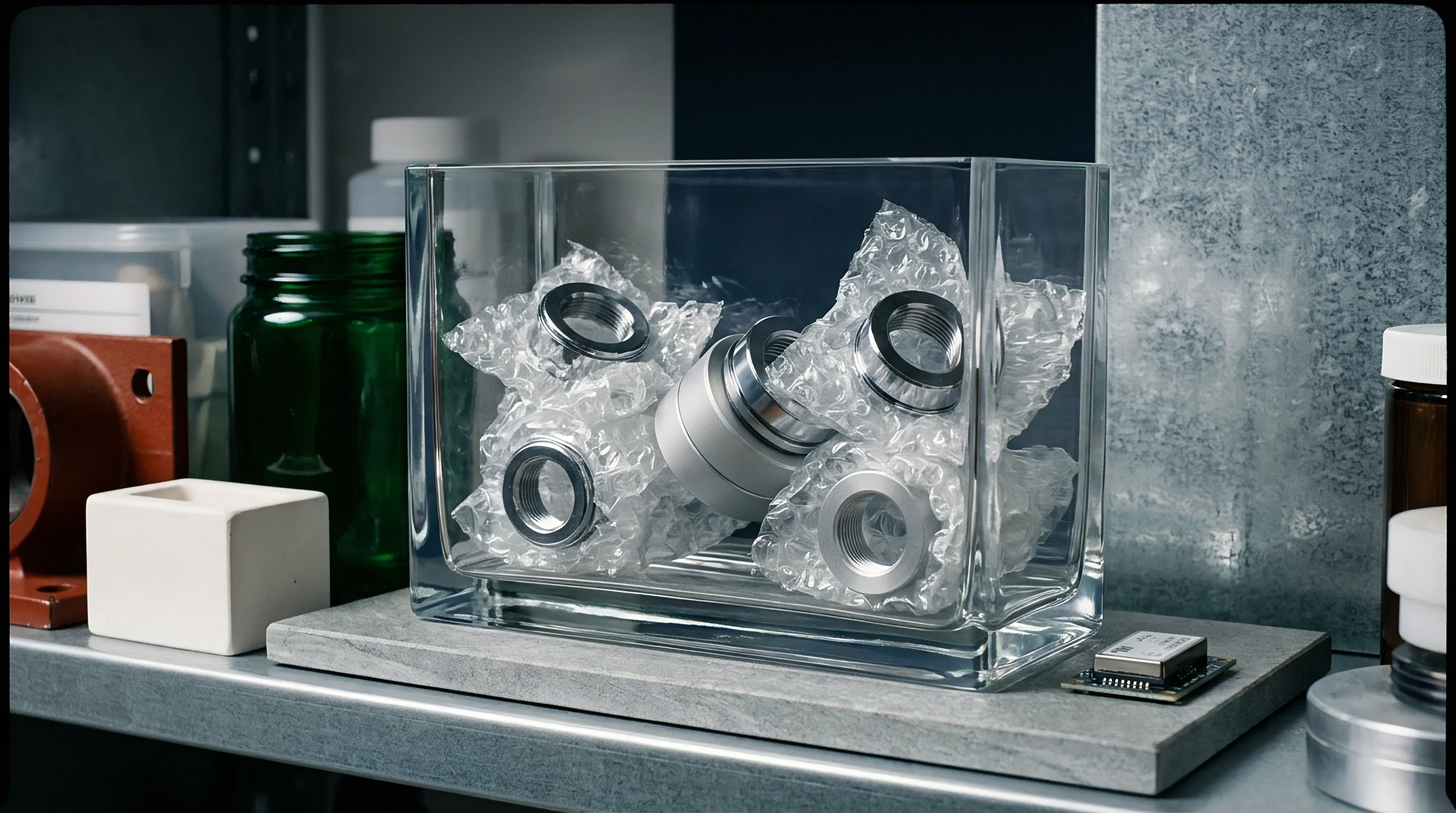
A rigorous inspection of incoming capacitive displacement probes must account for this coupled mechanism. Standard cleanroom packaging protocols using antistatic polyethylene bags inadvertently coat sensor electrodes with long-chain amides and slip agents. When introduced into an ultra-high vacuum test rig, these organic residues desorb slowly over months while providing deep surface traps for stray electrons.
The result is an uncontrolled drift rate that masks the true mechanical performance of the proof mass suspension.
Static charges trapped on internal alumina mounts alter the apparent mechanical stiffness of proof-mass suspensions via electrostatic force gradients that decay over thousands of vacuum hours.
A buyer who accepts factory calibration records conducted in ambient air incurs the full financial risk of this drift. When the cavity undergoes high-temperature bakeout and enters deep vacuum, the adsorbed air films desorb, shifting the zero point by tens of nanometers. Once operational, the subsequent slow accumulation of isolated charges continuously shifts the baseline, generating false alarms in structural health monitors or forcing manual recalibration cycles.
Operating a capacitive cavity without conductive grounding shields on every exposed dielectric surface guarantees an unpredictable baseline drift signature over long deployments.


Drift
Translating theoretical kinetic models into traceable displacement figures requires a systematic uncertainty budget. The Drift Investigator evaluates performance over a three-year timeline, tracking the decay of outgassing rates against the gradual accumulation of surface potential. Long-term stability cannot be confirmed by a four-week bench evaluation; the underlying time constants demand extended numerical modeling coupled with verified test checkpoints.

Worked Drift Analysis for an Inertial Sensing Cavity
Consider a representative ultra-high vacuum capacitive displacement sensor designed for seismic isolation or space-based reference tracking. The geometry consists of two parallel plate electrodes with an area A of 4.0 × 10⁻⁴ m2 (20 mm × 20 mm) separated by a nominal gap d0 of 1.0 mm (1.0 × 10⁻³ m). The nominal vacuum capacitance C0 is:
C0 = (epsilon0 A) / d0 = (8.854 × 10⁻¹² F/m × 4.0 × 10⁻⁴ m2) / (1.0 × 10⁻³ m) = 3.5416 pF
The readout electronics employ an interrogation bridge operating with an excitation voltage Vac of 5.0 V RMS at 100 kHz. Displacement sensitivity Sc is defined as:
Sc = dC / dd = – (epsilon0 A) / d02 = – 3.5416 pF / mm = – 3.5416 fF / micrometer
Assume the sensor housing is manufactured from vacuum-baked 304L stainless steel, supported by high-purity alumina isolators. Over a three-year mission profile (26,280 hours), three distinct physical mechanisms induce systematic drift in the demodulated displacement output:
- Water monolayer desorption phase ~ Over the first 150 hours, residual water desorbs from the gold-coated electrode faces, reducing the adsorbed layer thickness from 0.20 nm to zero. Assuming a relative dielectric permittivity of 6.0 for the bound water layer, the apparent capacitance shifts by -0.0028 fF. This corresponds to an apparent mechanical gap expansion of 0.79 nanometers.
- Ceramic charge accumulation phase ~ Secondary electrons from cosmic background radiation and field emission accumulate on unshielded alumina standoffs at an effective net current of 2.0 × 10⁻¹⁷ A. Over three years, the net charge reaches 1.89 × 10⁻⁹ C, inducing an average stray DC potential Vdc of 120 mV across the electrode perimeter. This DC field mixes with the carrier voltage, producing an electrostatic force and an offset that registers as an apparent 1.45 nanometer displacement drift.
- Surface patch potential evolution phase ~ Gradual migration of residual carbon monoxide across gold crystal boundaries alters the local work function distribution, shifting the mean contact potential difference by 45 mV between year one and year three. This contributes an additional 0.54 nanometers of baseline wander.
The total accumulated baseline displacement error delta dtotal over three years reaches:
delta dtotal = 0.79 nm + 1.45 nm + 0.54 nm = 2.78 nanometers
For an instrument with a specified stability requirement of 0.50 nanometers per year, this drift budget exceeds allowable limits if unmitigated. The vendor who quotes an initial resolution of 0.05 nanometers delivers an instrument that drifts by more than fifty times its resolution floor across its operational lifetime.
| Uncertainty Contribution Source | Standard Uncertainty (ui) | Probability Distribution | Sensitivity Coefficient (ci) | Uncertainty Contribution (nm) |
|---|---|---|---|---|
| Bridge Electronics Thermal Drift | 0.08 nm | Normal | 1.0 | 0.080 |
| Patch Potential Variation (Delta Phi) | 0.22 nm | Rectangular | 1.0 | 0.127 |
| Dielectric Charge Accumulation (Qstray) | 0.65 nm | U-Shaped | 1.0 | 0.460 |
| Adsorbed Layer Desorption Dynamics | 0.30 nm | Rectangular | 1.0 | 0.173 |
| Mechanical Frame Creep (Invar Mount) | 0.15 nm | Normal | 1.0 | 0.150 |
| Gas-Phase Density Fluctuation | 0.002 nm | Normal | 1.0 | 0.002 |
| Combined Expanded Uncertainty (k = 2) | — | Student-t | — | 1.084 nm |
The expanded uncertainty of 1.084 nanometers completely invalidates sub-nanometer long-term claims unless active charge discharging schemes or continuous Kelvin probe monitoring protocols are integrated into the cavity design. The uncertainty budget demonstrates that electrostatic charge accumulation on dielectrics represents the single largest contributor to measurement degradation, far exceeding mechanical thermal drift and bulk gas-phase variations.
Procuring capacitive sensors for mission-critical vacuum payloads requires moving past standard factory acceptance tests that only measure noise floor over ten-minute intervals. Acceptance documentation must stipulate minimum thermal soak durations, verify bakeout protocols, and establish baseline drift verification over hundreds of hours under certified vacuum conditions.
Failure to specify dielectric shielding configurations leaves the buyer exposed to baseline drift errors that cannot be corrected through digital filtering once the chamber is sealed.

Proofing
Mitigating outgassing kinetics and electrostatic accumulation requires explicit mechanical design controls, verified material preparation protocols, and active mitigation architectures. Passive prevention must be combined with active charge management to maintain sub-nanometer capacitive stability over multi-year deployments.

Mechanical and Surface Architecture Controls
To eliminate charge accumulation on dielectric insulators, design engineers isolate all insulating standoffs from direct line-of-sight to the sensing volume. Recessed ceramic geometries paired with conductive Faraday cages prevent charged particles from reaching high-resistivity surfaces. Metallic guard rings held at the same AC potential as the sensing electrode eliminate edge fringing fields, while auxiliary DC grounds drain static charges before potentials build up.
Material selection for electrodes demands strict metallographic control. Rather than generic electroplated gold over nickel strike, which develops interdiffusion boundaries and high pinhole densities, high-stability vacuum electrodes utilize sputtered high-purity gold or platinum thin films deposited over single-crystal silicon or ultra-low expansion glass-ceramics such as Zerodur. Polishing substrates to surface roughness Ra below 0.5 nanometers minimizes micro-asperities, reducing field emission currents by an order of magnitude.
Vacuum firing components at 1,073 K for 24 hours prior to final assembly drives out interstitial hydrogen from bulk metal lattices, permanently lowering baseline outgassing rates.

Active Charge Dissipation Methods
When passive shielding proves insufficient to suppress electrostatic buildup over long missions, active neutralization systems provide an operational defense. Three proven techniques serve ultra-high vacuum capacitive sensing cavities:
- Deep ultraviolet photo-discharge utilizes UV illumination (typically 254 nm from mercury lines or 265 nm from solid-state LEDs) directed at the sensing faces to liberate electrons via the photoelectric effect, neutralizing positive charge accumulations without physical contact.
- Periodic Kelvin probe force feedback modulates a small AC bias voltage on the guard electrodes to detect and continuously null the contact potential difference across the gap, canceling patch field forces dynamically.
- Conductive diamond-like carbon coating applied to ceramic isolation standoffs provides a controlled leakage resistance near 1011 ohms, which permits static charges to bleed to ground while preserving the high AC isolation impedance necessary for sub-femtosecond bridge detection.
Implementing deep ultraviolet photo-discharge introduces secondary complications that must be factored into the overall instrument budget. Continuous UV irradiation can stimulate the photolytic cracking of residual hydrocarbons, creating stubborn carbonaceous films on the gold electrodes. This shifts the permanent work function of the surface and introduces irreversible capacitance drift.
Active neutralization sequences must be deployed periodically during scheduled calibration windows, rather than run continuously.
From an operational standpoint, verifying an ultra-high vacuum capacitive sensor demands an incoming test dossier containing residual gas analysis spectra, work function uniformity maps, and electrostatic discharge time constant verifications. Standard commercial sensors lack this traceable documentation.
Contractual specifications must incorporate mandatory compliance clauses derived from ISO 14644-8 and ASTM E595 outgassing limits, amended to mandate CV-hysteresis testing under ultra-high vacuum to demonstrate freedom from surface trapping states before hardware delivery.