Die Attach Epoxy Degradation Mechanics in Microelectronic Packaging
Die attach epoxy degradation stems from thermal scission, moisture plasticization, and cyclic shear stress, requiring verified screening to ensure bondline stability.

Polymer
Microelectronic die attach adhesives rely on crosslinked thermosetting resin systems to maintain structural integrity under power cycling. Bisphenol A and Bisphenol F diglycidyl ether epoxies, combined with cycloaliphatic resins and novel novolacs, form the binder matrix for conductive and non-conductive adhesives. Thermal exposure during burn-in and service life initiates thermal oxidation within this matrix.
Oxidation breaks aliphatic chains, generates radical species, and alters the mechanical properties of the bondline. High temperatures accelerate these reactions, increasing elastic modulus while reducing strain capacity before fracture.
Thermal degradation manifests as chain scission, crosslink density increase, or secondary post-curing. During chain scission, thermo-oxidative cleavage breaks main-chain carbon-carbon and carbon-oxygen bonds, producing low-molecular-weight fragments. These fragments volatilize or remain trapped, acting as plasticizers that lower the glass transition temperature (Tg).
Post-curing occurs when residual unreacted epoxide groups react with active hydroxyls or residual amine curing agents at elevated temperatures. Post-curing raises Tg, embrittles the matrix, and builds internal residual stress across the die-substrate interface.
Higher crosslinking density improves high-temperature modulus while lowering strain capacity before brittle fracture.
The relationship between glass transition temperature drift and thermo-oxidative scission follows Arrhenius kinetics. Kinetic modeling relies on differential scanning calorimetry and thermogravimetric analysis to calculate the degradation activation energy (Ea). Typical activation energies for electronics-grade silver-filled epoxies range from 85 kJ/mol to 130 kJ/mol.
When elevated temperatures drive the glass transition temperature above the maximum package operating limit, the adhesive shifts from a viscoelastic state to a rigid, glassy state. This shift increases storage modulus (E’) from 1.5 GPa up to 8.5 GPa, drastically increasing interfacial shear stress during thermal cycling.

Thermo-Oxidative Degradation of Thermosetting Matrices
Thermo-oxidative scission depends on oxygen diffusion into the thin bondline. At die edges, oxygen ingress reacts with methylene carbons adjacent to ether linkages. Radical reactions form hydroperoxides, which decompose into alkoxy radicals, leading to carbonyl and carboxylic acid formation.
Infrared spectroscopy tracks this degradation through the growth of the carbonyl absorption peak at 1720 cm-1 relative to the invariant aromatic reference peak at 1608 cm-1. The resulting loss of cohesive strength creates localized micro-cracks along the die periphery.
- Thermo-oxidative scission breaks carbon-carbon backbones under high operating temperatures, reducing adhesive cohesive strength over operational lifetimes.
- Volatilization of diluents releases low-molecular-weight reactive diluents during high-temperature dwell, inducing volumetric shrinkage and bondline stress.
- Filler-matrix debonding disconnects conductive silver flakes from oxidized epoxy chains, increasing electrical contact resistance across the die backing.
- Catalyst residue breakdown generates acidic fragments at elevated temperatures, accelerating corrosion along silver-plated leadframe surfaces.

Glass Transition Temperature Drift and Crosslink Scission
Changes in Tg directly govern thermal stress development across the silicon-substrate stack. Dynamic mechanical analysis measures storage modulus, loss modulus (E”), and loss factor (tanδ) across temperature sweeps. A positive Tg shift indicates post-curing, which elevates room-temperature residual stress.
A negative Tg shift indicates polymer network degradation through main-chain scission or hygral plasticization. Adhesives exhibiting a Tg shift greater than ± 10circC after 1,000 hours of High Temperature Operating Life (HTOL) testing at 150circC demonstrate unstable matrix kinetics, predisposing packages to early interfacial delamination.
Post-curing matrix embrittlement stems either from lot-level variations in monomer purity or improper ramp rates during oven curing.

Void
Entrapped gases and solvent vapors during die attach cure create localized gaps in the bondline structure. Voids lower effective heat dissipation area, causing localized die hot spots that accelerate active silicon junction degradation. Outgassing kinetics govern void growth during cure ramp steps.
Solvent-borne epoxies retain diluents if the ramp rate exceeds the evaporation threshold. Fast temperature ramps skin over the adhesive surface, trapping volatile solvents beneath a polymerized top layer.
Voiding mechanics involve bubble nucleation, growth, and coalescence driven by internal vapor pressure. Unreacted monomers, reactive diluents, and absorbed ambient moisture vaporize when cure temperatures cross their boiling thresholds. Entrapped bubbles coalesce into macro-voids under large-area power dies.
Macro-voids spanning more than 15 percent of the total die area create severe thermal impedance gradients. The local junction temperature (Δ Tj) rises proportionally to the reduction in conductive path cross section.
| Epoxy Matrix Type | Filler Material | Thermal Conductivity (W/m·K) | Total Mass Loss (%) | Collected Volatile Condensable Material (%) | Glass Transition Temperature Tg (°C) |
|---|---|---|---|---|---|
| Silver-Filled Bisphenol F | Ag Flake (75-80 wt%) | 2.5 – 4.0 | 0.35 | 0.02 | 120 |
| High-Thermal Conductive Hybrid | Ag + Sintered Micron Powder | 8.0 – 15.0 | 0.18 | 0.01 | 165 |
| Non-Conductive Silica-Filled | SiO2 Spheres (60-70 wt%) | 0.8 – 1.2 | 0.45 | 0.04 | 140 |
| Anhydride-Cured Novolac | Ag Flake (82 wt%) | 3.0 – 5.5 | 0.12 | 0.005 | 185 |

Outgassing Kinetics and Solvent Retention
Standard outgassing assessments rely on ASTM E595 testing. The protocol subjects cured adhesive samples to 125circC under a vacuum of 5 × 10⁻⁵ torr for 24 hours. Space-grade microelectronics specify a Total Mass Loss (TML) below 1.0 percent and Collected Volatile Condensable Material (CVCM) below 0.10 percent.
High TML values indicate incomplete cure, excess unreacted diluents, or thermal decomposition of catalyst residues. Volatiles released inside hermetic or ceramic packages condense on wire bonds and optical sensors, inducing bond pad corrosion or optical clouding.
Thermal Impedance Spikes across Bondline Discontinuities
Voids alter heat flux vectors inside semiconductor packages. Fourier’s law of heat conduction dictates that heat flow distributes uniformly across solid, void-free interfaces. Interfacial gaps act as thermal insulators, squeezing heat flux lines into adjacent solid epoxy regions.
Thermal resistance (Rth) increases non-linearly with void percentage.
Large voids located directly beneath high-power density regions (such as power MOSFET channels or RF amplifier gates) cause localized junction temperature spikes of up to 25circC above baseline thermal modeling projections. This temperature spike accelerates local thermo-oxidative matrix degradation, creating a runaway failure mechanism where thermal resistance and matrix breakdown continuously reinforce each other.
Exceeding five percent total bondline area loss at die corners accelerates edge delamination during subsequent thermal assembly steps.

Moisture
Ambient water vapor penetrates plastic encapsulated microcircuits through the bulk molding compound interface. Water molecules diffuse through the polymer network via Fickian diffusion mechanics, collecting at internal material boundaries. Moisture accumulation inside die attach epoxies causes plasticization, glass transition temperature suppression, and loss of interfacial adhesion strength.
Water molecules interrupt hydrogen bonds between epoxy hydroxyl groups and substrate oxide layers, substituting low-strength water-epoxy bonds.
Plasticization increases polymer chain mobility, lowering elastic modulus and shifting the glass transition temperature downward by as much as 20circC to 40circC under high humidity exposure. Moisture absorption efficiency depends on ambient relative humidity and temperature, reaching equilibrium saturation per non-steady-state diffusion laws:
C(x,t) = Csat left
where Csat is saturation moisture concentration, D is the temperature-dependent diffusion coefficient (D = D0 exp(-Ed / RT)), x is diffusion depth, and t is exposure duration.
An adhesive matrix exposed to 85°C and 85 percent relative humidity loses up to 35 percent of its initial die shear strength within 168 hours.
Rapid temperature increases during reflow soldering (reaching 245circC to 260circC) vaporize trapped moisture instantaneously. Hydrostatic vapor pressure inside microscopic voids and delaminated interfaces scales according to the ideal gas law and saturation vapor pressure dynamics, exceeding 4.0 MPa at reflow temperatures. If vapor pressure exceeds the localized hot-die-shear strength of the moisture-softened adhesive, the bondline ruptures.
This phenomenon, known as popcorn cracking, generates catastrophic delamination across the die attach plane.

Hygral Plasticization and Tg Suppression
Absorbed moisture alters the mechanical constitutive properties of silver-filled epoxies. Swelling induced by water absorption introduces hygral strain (εm = β · Δ C), where β is the coefficient of moisture expansion (CME) and Δ C is concentration change. When hygral expansion of the adhesive conflicts with low-expansion silicon dies (α ≈ 2.6 p±/K) and high-expansion copper leadframes (α ≈ 17 p±/K), severe interfacial shear stresses emerge even without thermal gradients.
| Moisture Sensitivity Level (J-STD-020) | Floor Life Condition | Soak Test Condition | Die Shear Strength Loss Post-Soak (%) | Interfacial Delamination Risk |
|---|---|---|---|---|
| MSL 1 | Unlimited at ≤30°C / 85% RH | 168 hrs at 85°C / 85% RH | < 10 | Low |
| MSL 2 | 1 Year at ≤30°C / 60% RH | 168 hrs at 85°C / 60% RH | 10 – 20 | Moderate |
| MSL 3 | 168 Hours at ≤30°C / 60% RH | 192 hrs at 30°C / 60% RH + 40 hrs 60°C | 20 – 35 | High |
| MSL 4 | 72 Hours at ≤30°C / 60% RH | 96 hrs at 30°C / 60% RH + 20 hrs 60°C | 35 – 50 | Critical |
Popcorn Cracking and Interfacial Steam Pressure
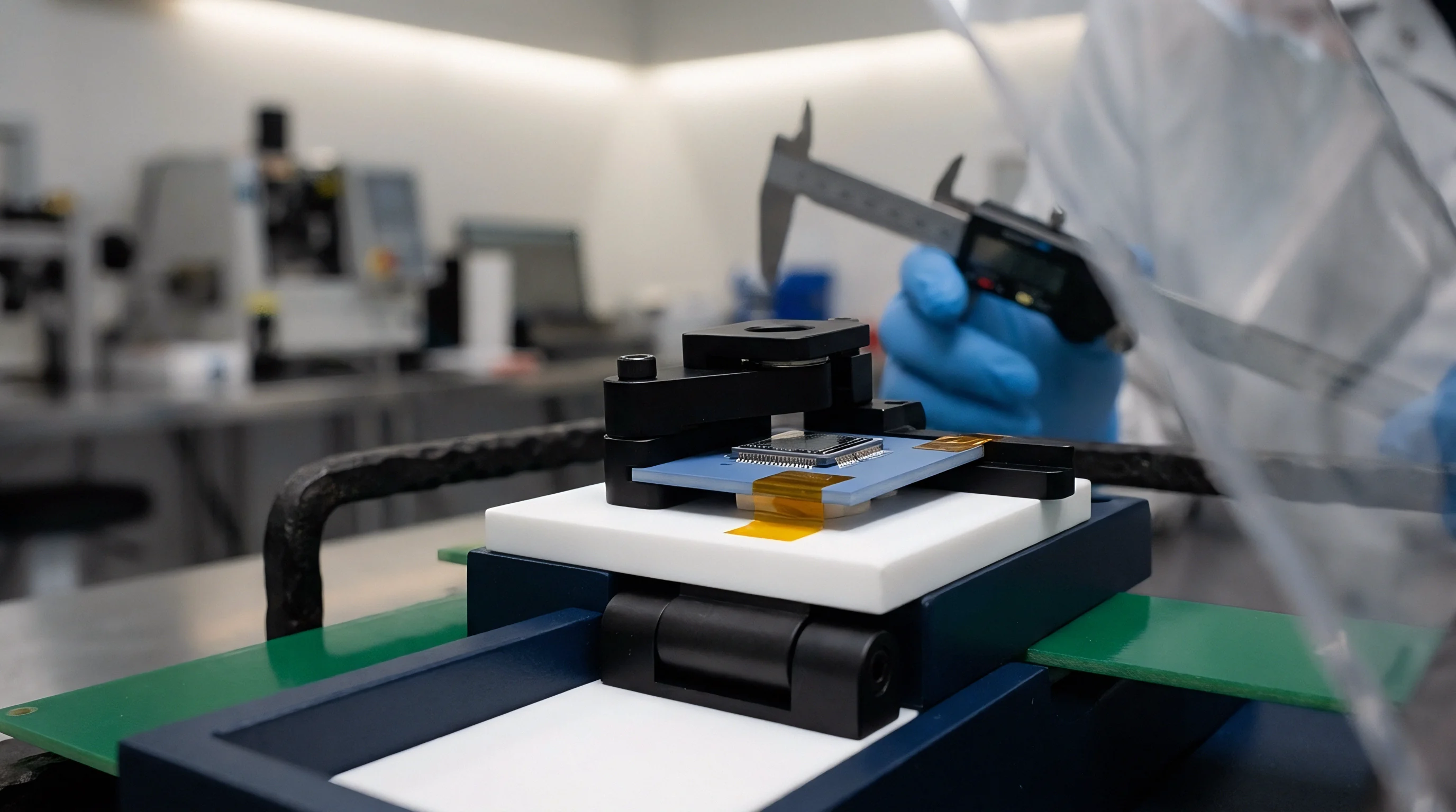
Vapor-driven delamination initiates at high-stress concentration zones, primarily die corners and edge fillets. Hydrostatic pressure forces the delamination front to propagate inward along the weakest interface (typically the die-to-epoxy boundary if silver-plating adhesion is optimized). High temperature during reflow accelerates adhesive strength degradation simultaneously.
If the hot shear strength drops below 1.5 MPa at 250circC, total structural collapse of the die bond line occurs during package mounting.
Uncontrolled package storage outside vapor-barrier packaging drives internal steam generation during reflow, splitting interfacial bonds and generating high field return costs.


Fatigue
Thermal expansion differentials between silicon dies and metallic leadframes induce cyclic shear strains within the adhesive layer. Operating microelectronics undergo power-cycling and environmental temperature changes, subjecting the bondline to low-cycle thermal fatigue. Coefficient of thermal expansion (CTE) mismatch between silicon (≈ 2.6 p±/K), direct bonded copper substrates (≈ 6.8 p±/K), and standard copper leadframes (≈ 16.5 p±/K) generates continuous shear strain profiles along the adhesive layer during thermal swings.
Plastic shear strain per cycle (Δ γp) maps directly to fatigue life through the Coffin-Manson relation:
Nf = C left( Δ γp right)-n
where Nf is cycles to failure, C is a material ductility constant, and n is the fatigue exponent (typically ranging between 1.5 and 2.5 for silver-filled epoxies). Creep deformation accelerates during high-temperature dwell steps, converting elastic strain into irreversible plastic shear deformation.
JESD22-A104 condition G mandates temperature cycling between -40°C and +125°C, where mismatched thermal expansion coefficients initiate delamination at die corners.
The physical distribution of shear stress along a die attach bondline follows Suhir’s solution for tri-layer assemblies. Shear stress (τ) concentrates exponentially at die edges, reaching maximum value (τmax) within a distance equal to two bondline thicknesses from the die edge:
τmax = fracΔ α · Δ T · Gκ tanh(κ · L)
where Δ α is CTE mismatch, Δ T is temperature change, G is adhesive shear modulus, L is half die length, and κ is the interfacial compliance parameter. Larger die dimensions scale edge stress non-linearly, making 10 mm × 10 mm power dies significantly more vulnerable to corner fatigue cracking than 2 mm × 2 mm signal dies.

Thermo-Mechanical Mismatch across Package Interfaces
Repeated thermal cycling generates alternating shear displacement across the bondline. Below Tg, the high modulus of the adhesive transmits large thermal stress directly to the silicon die, risking die cracking. Above Tg, modulus drops dramatically, shifting the stress relief mechanism into plastic deformation of the adhesive.
High strain rates during rapid thermal ramps inhibit creep relaxation, forcing the material into brittle stress regimes that initiate micro-fractures within the filled polymer matrix.
- Corner shear accumulation focuses maximum thermal strain at die peripheries where spatial distance from the die center reaches its extreme.
- Interfacial creep relaxation shifts strain distributions during steady high-temperature dwell cycles, weakening matrix-to-substrate boundary layers.
- Fillet micro-cracking initiates along high-stress adhesive meniscus edges and propagates inward under repeated temperature excursions.
- Substrate oxidation growth degrades metallic plating adhesion when oxygen diffuses through micro-fractured resin interfaces over time.

Crack Propagation Mechanics and Cohesive Failure
Micro-cracks originate at die corners, propagating inward along silver-flake pathways. Fracture mechanics models characterize this growth using the strain energy release rate (GI/II). Mixed-mode fracture (combining tensile opening Mode I and shear sliding Mode II) dominates corner delamination behavior.
As micro-cracks grow, thermal resistance increases while effective load-bearing area drops. When crack lengths reduce the intact bond area by 20 to 30 percent, thermal dissipation fails catastrophically, inducing die burnout during high-power operation.
When Does Thermal Mismatch Trigger Interfacial Fracture?
Interfacial fracture occurs when the driving strain energy release rate exceeds the critical interfacial fracture toughness (Γic). Toughness depends on surface preparation, substrate oxidation, and clean metal plating. Oxygen plasma cleaning before die attach increases initial surface energy, elevating Γic from 25 J/m2 to over 80 J/m2.
Thermal aging degrades surface energy by building brittle intermetallic compounds and copper oxides (Cu2O and CuO) beneath the adhesive layer, lowering critical fracture resistance over operational lifespans.
Whether low-stress silicone-modified formulations can prevent interfacial fatigue failure without introducing unacceptably high die tilt remains unresolved across high-power automotive modules.

Screening
Non-destructive acoustic evaluation and destructive shear testing quantify structural integrity before components enter assembly lines. Screening protocols establish baseline parameters for void distribution, delamination area, and cohesive shear strength across incoming component lots. Calibration of non-destructive screening tools relies on traceable physical standards containing laser-etched air gaps of known lateral and vertical dimensions.
C-Mode Scanning Acoustic Microscopy (C-SAM) utilizes high-frequency ultrasound (typically 50 MHz to 230 MHz) to detect interfacial discontinuities. Acoustic impedance (Z = ρ · v, where ρ is density and v is sound velocity) dictates ultrasound reflection at material interfaces. The reflection coefficient (R) between two media is expressed as:
R = fracZ2 – Z1Z2 + Z1
At a solid epoxy (Z1 ≈ 3.0 × 10⁶ kg/m2s) to air void (Z2 ≈ 400 kg/m2s) interface, R approaches -1.0. This total reflection produces a 180-degree acoustic phase inversion, revealing voids, cracks, and delaminations as high-contrast bright features in C-SAM acoustic images.
Transient thermal resistance measurements identify subsurface adhesive delamination long before acoustic microscopy detects micro-crack propagation.
Destructive physical verification relies on die shear strength testing per MIL-STD-883 Method 2019. A calibrated contact tool applies a uniform lateral force against the die edge until structural bond separation occurs. Test standards define minimum acceptable shear force based on total die contact area.
Post-test examination under optical microscopy determines failure mode classification: cohesive failure within the epoxy matrix, adhesive failure at the die-epoxy interface, or substrate plating detachment.

C-Mode Scanning Acoustic Microscopy and Acoustic Impedance Maps
High-frequency acoustic transducers determine vertical resolution within multi-layer microelectronic packages. A 100 MHz transducer delivers a lateral spatial resolution of approximately 15 μm, while a 230 MHz transducer resolves features down to 5 μm. Operating at higher frequencies increases acoustic attenuation within thick mold compounds, requiring custom acoustic lens selection based on package depth.
Quantitative acoustic screening calculates total voided area percentages automatically via digital image phase thresholding algorithms.
| Metrology Method | Primary Failure Mode Detected | Destructive Status | Spatial / Measurement Resolution | Throughput Speed |
|---|---|---|---|---|
| C-Mode SAM (100-230 MHz) | Delamination, Voids, Micro-cracks | Non-Destructive | 5 µm – 15 µm lateral | Low to Moderate (Batch) |
| X-Ray Tomography (3D XCT) | Volumetric Voids, Silver Settling | Non-Destructive | 1 µm – 3 µm voxel size | Very Low (Offline Audit) |
| Die Shear Strength (MIL-883) | Adhesive / Cohesive Bond Weakness | Destructive | ± 0.05 N shear force | High (Sample Lot) |
| Transient Thermal Resistance | Thermal Path Degradation, Tilt | Non-Destructive | ± 0.01 K/W thermal impedance | High (Automated In-Line) |

Transient Dual Interface Thermal Resistance Characterization
Transient thermal testing measures structure functions per JESD51-14. By comparing cumulative thermal impedance (Zth) curves of a component measured with two different thermal interface materials against a cold plate, metrologists identify the exact point where thermal path variability originates. The point of separation between the two cumulative thermal resistance profiles pinpoints the physical location of the die attach layer.
A upward shift in the thermal capacitance-resistance curve indicates localized delamination or excessive bondline thickness (BLT) variance.
Bondline thickness variations exceeding ± 20 percent across a single large power die induce non-uniform thermal dissipation profiles, increasing localized thermal stress. In-line transient thermal measurement screens 100 percent of power module production lots without subjecting packages to mechanical stress.
- Position the packaged semiconductor device inside the liquid immersion tank of the ultrasonic acoustic microscope.
- Align the high-frequency transducer focus plane at the interface between the silicon die back surface and adhesive layer.
- Capture reflection amplitude maps across the die bond area to identify localized acoustic phase inversions.
- Quantify total contiguous phase-inverted regions as a percentage of overall die footprint area.
MIL-STD-883 Method 2019 defines minimum die shear force thresholds based on die surface area, governing mechanical acceptance for military-grade microcircuits.

Audit
Qualification protocols for high-reliability semiconductor packaging demand verified physical dossiers on adhesive formulations and cure schedules. Sourcing high-performance die attach materials involves verifying supplier data sheets against bench test results. Datasheet claims regarding thermal conductivity and outgassing percentages often rely on idealized laboratory test conditions that differ significantly from production assembly line realities.
Yield loss from die attach failure compounds as components move through downstream manufacturing steps. Scrap costs incurred at final functional test exceed bare die attach process costs by orders of magnitude. Quality audits verify material lot consistency, shelf-life storage compliance (typically -40circC storage with strict freeze-thaw cycle limits), and differential scanning calorimetry (DSC) cure kinetics data for every incoming batch.
Supplier Dossier Verification and ASTM E595 Outgassing Compliance
Quality engineers review chemical characterization dossiers before approving new adhesive formulations. Chemical dossiers include Fourier Transform Infrared (FTIR) spectra footprints, gel time curves, and thermogravimetric analysis (TGA) degradation curves. Auditing incoming adhesive lots prevents sub-standard material batches from entering automated dispensing lines.
Viscosity drift over working life windows (pot life) alters dispense dot geometry, leading to irregular fillet height, bondline voiding, and die tilt.
- Cure schedule validation verifies differential scanning calorimetry profiles to ensure total chemical conversion exceeds 98 percent for incoming material lots.
- Outgassing certified limits checks total mass loss below 1.0 percent and collected volatile condensable material below 0.10 percent per ASTM E595 guidelines.
- Rheological consistency checks measure viscosity drift across working life windows to prevent bondline thickness variation on automated assembly lines.
- Bondline thickness verification confirms post-cure adhesive height matches thermal resistance modeling assumptions across all production lots.

Commercial Economics of High-Reliability Die Attach Sourcing
Specifying high-reliability die attach adhesives requires balancing material unit costs against potential warranty liability. Standard commercial silver-filled epoxies cost approximately $0.50 to $1.50 per gram. Advanced silver-sintering pastes and ultra-high thermal conductivity hybrid epoxies range from $5.00 to $15.00 per gram.
However, high-reliability materials reduce long-term field return rates in automotive, aerospace, and power grid applications where single system failures incur catastrophic field replacement penalties.
A rigorous material audit sequence validates chemical stability, moisture sensitivity, outgassing limits, and thermo-mechanical fatigue resistance across the package service life. Establishing direct analytical verification steps prevents supplier material variations from compromising final packaged semiconductor reliability.