Mechanical Loading
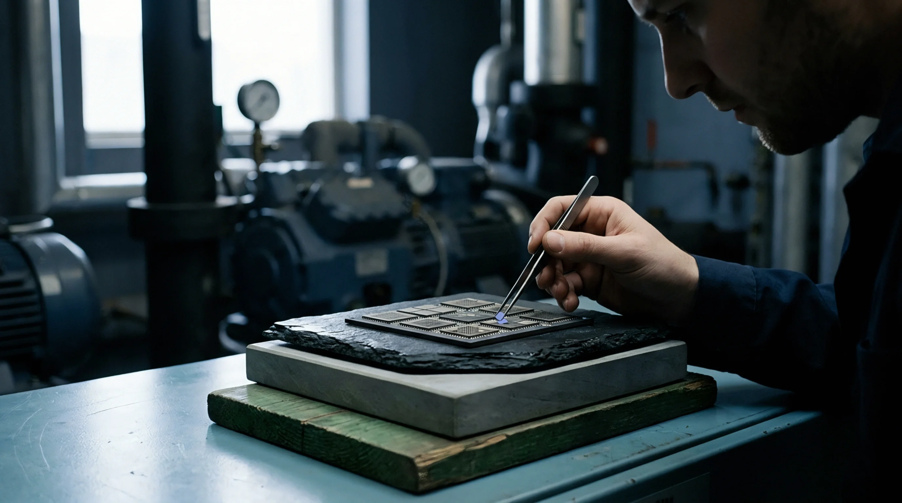
Physical strain experienced by wafer-level semiconductor packages arises from the direct mounting of the silicon die onto a printed circuit board using solder bumps. Since there is no intermediate lead frame or plastic molding, wlcsp stress is transferred directly from the board into the silicon crystal lattice. This mechanical force is caused by the mismatch in the coefficients of thermal expansion between the rigid silicon and the organic board material.
During temperature changes, this mismatch exerts bending and shear forces on the microscopic solder bumps.
Package Reliability
Package reliability is compromised when these shear forces cause solder fatigue and cracking over repeated thermal cycles. The absence of a protective plastic housing leaves the edges of the silicon die vulnerable to micro-cracking and chipping during assembly. To ensure long-term survivability, manufacturers perform drop testing and thermal shock evaluation to characterize the mechanical durability of the connections.
These tests identify the boundaries of the package’s resistance to mechanical failure.
Electrical Drift
The electrical drift caused by this physical strain occurs through the piezoresistive effect, which alters the mobility of charge carriers within the silicon. When stress is applied to the die, the resistance of integrated resistors and the offset voltage of differential pairs shift from their calibrated values. This shift directly degrades the accuracy of high-resolution analog-to-digital converters and precision voltage references.
Designers observe this drift as a non-linear shift in performance during board assembly and reflow. This behavior requires careful layout considerations, such as placing the chip away from mounting holes and board edges where mechanical bending is most pronounced, to ensure that the stress-induced analog offsets remain within the system’s design tolerance.
Mitigation Strategy
Mitigation strategy for this mechanical vulnerability involves the use of underfill materials to distribute stress across the package footprint. These liquid epoxies are applied under the die and cured to form a strong bond that reduces the shear load on the solder bumps. This physical reinforcement prevents the board’s thermal expansion from translating directly into stress on the silicon die, thereby maintaining the long-term calibrated precision of the analog circuit.