Thermal Gradient Induced Offset Drift in Package Reflow Operations
Differential reflow heating creates asymmetric mold compound strain, driving permanent microvolt zero-point offset drift across surface-mount sensor ICs.


Solder
Surface-mount assembly lines expose integrated circuit packages to peak profile temperatures between 245 °C and 260 °C during lead-free reflow operations. When printed circuit board assemblies pass through multi-zone reflow ovens, radiant infrared emitters and forced convection gas streams transfer kinetic heat into the exposed packaging surfaces, leadframes, and underlying copper planes. Thermal mass variations across the board layout create localized temperature differentials across opposite sides of a single sensor package.
A small land pattern situated adjacent to heavy ground planes or solid power vias experiences a thermal lag compared to leads connected to isolated trace runs. This temperature differential across the package body induces non-uniform expansion across the internal leadframe, substrate, die-attach adhesive, and silicon die.
During the reflow cooling phase, solder joints solidify at the liquidus threshold of SAC305 alloy near 217 °C. Liquidus transitions lock in the instantaneous physical dimensions of the board and package. If a lateral temperature gradient of 3 °C to 8 °C exists across a 3×3 mm Quad Flat No-lead (QFN) or Land Grid Array (LGA) footprint during solidification, the solder joints freeze sequentially rather than simultaneously. The first joints to cool fix one side of the package into a rigid mechanical state while the opposite side continues to contract through thermal cooling.
This sequential locking creates frozen-in shear forces across the solder balls or perimeter leads. The die inside the package experiences an asymmetrical mechanical stress field that directly alters internal sensor Wheatstone bridge balance or operational amplifier transistor matching.
Reflow profiles maintaining a peak lead-to-body thermal gradient below 4 °C across a 3×3 mm LGA footprint limit immediate post-cooling baseline offset shifts to less than 0.15 millivolts per volt.
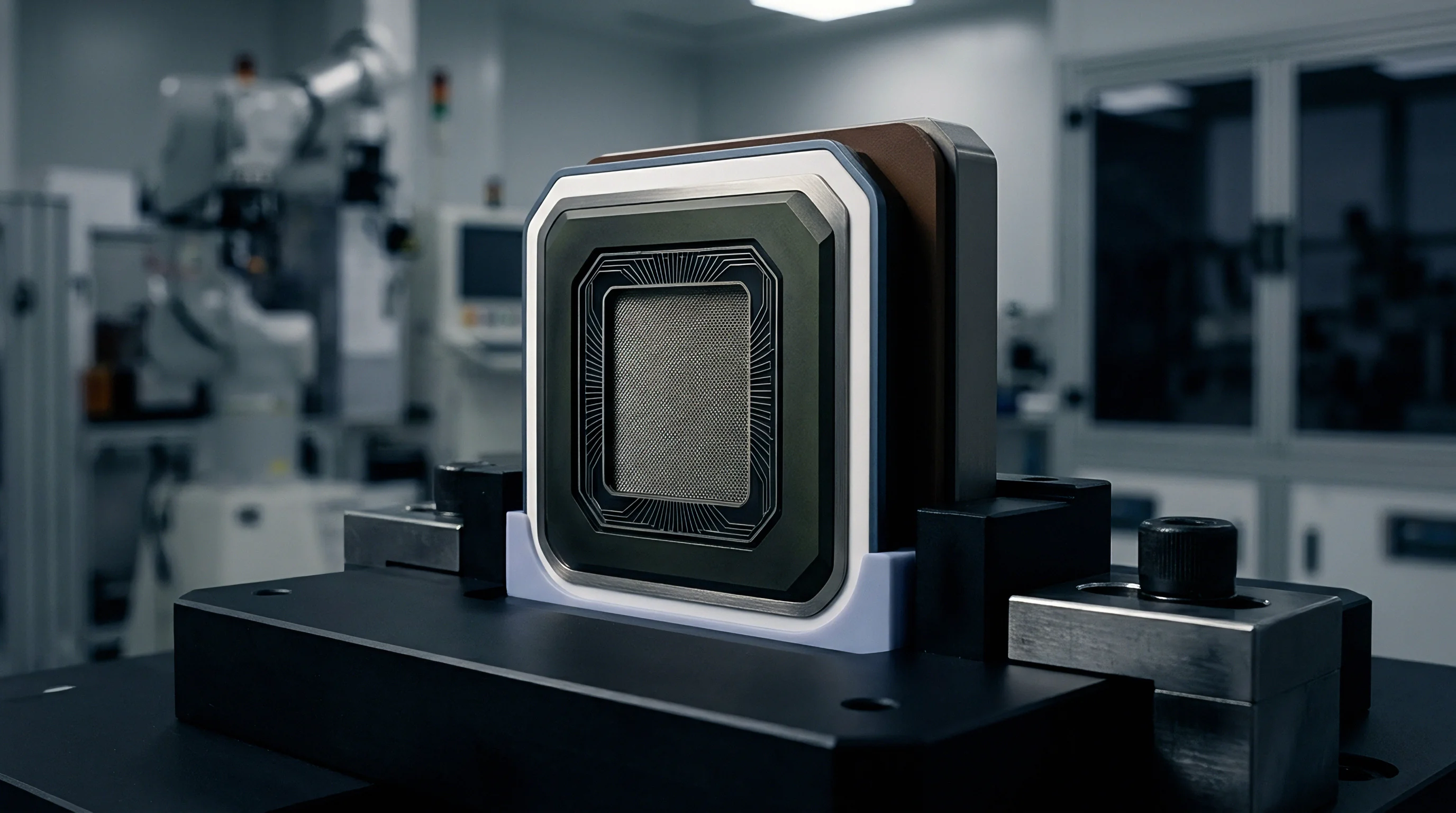
Thermal Inhomogeneity across Reflow Zones
Convection reflow ovens attempt to maintain uniform lateral temperature profiles across the conveyor belt width. Atmospheric turbulence, heater bank spacing, and edge loss effects create cross-belt thermal variances up to 5 °C. Board assemblies traversing the furnace experience dynamic temperature shifts between the top encapsulation mold surface and the bottom copper ground plane. Heavy inner copper layers act as heat sinks, retarding the ramp rate of bottom-terminated pads relative to top-side plastic mold compounds.
Peak thermal ramp rates exceeding 2.5 °C per second widen the internal temperature delta between the silicon substrate and the outer epoxy casing.
Asymmetrical thermal absorption across package boundaries induces micro-scale mechanical twisting during the liquid-to-solid phase transition of the solder alloy. When perimeter leads freeze while the central exposed thermal pad remains molten, the package experiences an upward or downward tilt relative to the PCB plane. Micro-tilting shifts the mechanical neutral axis of the die-attach surface.
Mechanical strain profiles captured via optical interferometric profilometry show that a tilt angle of just 0.04 degrees across a 4×4 mm DFN package translates to a 12 megapascal differential stress concentration along the active silicon edge.
The operational outcome manifests immediately during initial electrical testing on the line. Sensor channels report an uncalibrated baseline offset shift far exceeding the nominal factory calibration window. Post-assembly baseline shifts often stem from internal mold compound CTE anisotropy rather than improper reflow ramp rates alone.

Differential Heat Absorption in Asymmetric Land Patterns
Layout geometry controls the rate of thermal delivery into individual package pins during soldering profiles. Asymmetric copper land patterns create local thermal sinks that draw heat away from specific terminals faster than their opposing counterparts. Connecting pin one directly to a 2-ounce copper power plane while leaving pin four on a 5-mil signal trace establishes a persistent thermal gradient across the chip carrier throughout the reflow window.
Thermal imaging confirms that such layout asymmetry produces pin-to-pin temperature splits exceeding 6 °C at the precise instant of solder alloy solidification.
- Asymmetric Solder Freeze Sequential joint solidification locks structural shear stress into the package interface, generating unbalanced bending moments across the internal silicon element.
- Thermal Shadowing Large passive components or tall electrolytic capacitors placed upstream on the conveyor belt block convective airflow, reducing localized reflow temperatures on adjacent sensor package edges.
- Substrate Layer Distortion Differential expansion between top-layer signal traces and internal ground planes forces the PCB substrate to warp locally under the component footprint during peak reflow.
- Die-Attach Voiding Non-uniform heat distribution causes volatile solvents in die-attach adhesives to outgas unevenly, creating structural voids that alter internal heat transfer paths.
Resolving these mechanical imbalance vectors requires structural adjustments to the PCB footprint layout. Implementing thermal relief spokes on all plane-connected lands equalizes heat transfer rates between adjacent terminals. Equalizing pad thermal capacities reduces joint solidification delays down to less than 50 milliseconds across all terminals.
Solder-joint stress drops accordingly, preserving factory zero-point alignment specifications.


Warpage
Mechanical strain generated by mismatched thermal expansion coefficients alters the electrical behavior of integrated silicon transducers. A surface-mount sensor package constitutes a multi-material stack comprising silicon die, gold or copper wire bonds, die-attach epoxy, a copper leadframe or BT-laminate substrate, and an epoxy mold compound. Silicon exhibits a coefficient of thermal expansion (CTE) of approximately 2.6 ppm/K. Copper leadframes expand at 16.5 ppm/K. FR-4 substrate materials expand laterally at 14 to 17 ppm/K. Epoxy mold compounds display CTE values ranging from 10 to 25 ppm/K below their glass transition temperature, rising rapidly to 60 ppm/K above that threshold.
During cooling from peak reflow temperatures, each material layer contracts at a rate governed by its specific CTE and elastic modulus. Because the layers are rigidly bonded, differential contraction forces the entire assembly to bow or twist. Piezoresistive elements diffused into the silicon surface respond directly to this structural deformation.
The piezoresistive effect transforms mechanical strain into changes in electrical resistivity. A strain differential of 100 microstrain across a Wheatstone bridge array alters the output voltage balance by several hundred microvolts per volt of excitation.
| Material Layer | Coefficient of Thermal Expansion (ppm/K) | Modulus of Elasticity (GPa) | Glass Transition Temperature (°C) | Offset Sensitivity Impact |
|---|---|---|---|---|
| Monocrystalline Silicon Die | 2.6 | 130 – 169 | N/A | Primary piezoresistive transducer element |
| Copper Leadframe (C19400) | 16.5 | 121 | N/A | High thermal expansion differential vs silicon |
| BT-Laminate Package Substrate | 12 – 15 | 24 | 170 – 215 | Bending moment source under BGA/LGA forms |
| Epoxy Mold Compound (Standard) | 10 – 25 (below Tg) / 60 (above Tg) | 15 – 28 | 120 – 160 | Volumetric shrinkage drives package warpage |
| Die-Attach Adhesive (Silver Conductive) | 35 – 55 | 3.5 – 8.0 | 60 – 110 | Absorbs or transfers substrate strain to die |
| FR-4 Printed Circuit Board | 14 – 17 | 18 – 22 | 130 – 180 | External constraint forcing PCB-level flexure |

Thermomechanical Stress Coupling to Piezoresistive Structures
Stress fields imposed on the silicon die alter electrical performance through crystallographic axis deformation. Sensor designs orient piezoresistors along specific crystal planes such as the 110 direction in crystal silicon to maximize sensitivity to intended physical inputs. External strain vectors introduced by package flexure project components onto these exact crystal planes.
Shear stresses acting along the die diagonal create differential resistance changes across opposing bridge arms, generating a permanent uncalibrated zero-point offset error.
Under JEDEC JESD22-A104 condition B thermal profiling following SAC305 reflow, 3×3 mm LGA pressure sensors on standard 1.6 mm FR-4 four-layer test cards exhibit a zero-point offset shift of 0.82 mV/V. Increasing PCB copper weight from 1 oz to 2 oz or altering stencil thickness from 125 µm to 100 µm moves this value by up to 35 percent. Unsymmetric copper distribution on internal PCB layers amplifies localized board curvature under thermal load. The resulting strain state transfers directly through the solder joints into the package substrate, bending the silicon element.
Neglecting copper pour symmetry under sensitive MEMS land patterns leads to field recalibration failures and costly board-level rework across high-density production runs.

Coefficient of Thermal Expansion Mismatches in Substrate Stacks
Substrate stack behavior depends heavily on the relative thickness and elasticity of each bonded material layer. When the epoxy mold compound cools through its glass transition temperature, its volumetric shrinkage rate accelerates dramatically. The mold compound contracts faster than the underlying copper leadframe, exerting a upward pulling force along the package top surface.
This differential force induces a concave package deformation pattern commonly classified as smiley-face warpage.
Concave flexure stretches the upper silicon die face while compressing the lower die face. Compressively strained silicon exhibits altered carrier mobility, shifting transistor threshold voltages in analog front-end circuits. Operational amplifier offset voltages drift by several millivolts when differential pair transistors experience unequal compressive stress states.
Aligning layout features to minimize mechanical strain vectors remains mandatory for analog accuracy.


Hysteresis
Polymer components inside plastic integrated circuit packages exhibit time-dependent mechanical relaxation following high-temperature reflow processing. Epoxy mold compounds and organic die-attach adhesives are viscoelastic materials. At room temperature, their internal polymer networks exist in a metastable mechanical equilibrium.
Subjecting these materials to 260 °C peak reflow temperatures breaks temporary inter-chain bonds and alters the cross-linking density. As the package cools, internal residual stresses do not settle instantly to their final equilibrium values.
Viscoelastic creep causes internal package strain to decay exponentially over time following reflow processing. Immediate post-assembly zero-point offset measurements differ substantially from readings taken 72 hours later. The baseline offset drifts continuously as the epoxy matrix gradually relaxes its internal shear stresses.
This long-term baseline movement complicates factory calibration procedures on high-throughput surface-mount manufacturing lines.
Violating JEDEC J-STD-020 peak body temperature limits by 5 °C accelerates polymer mold compound cross-linking degradation and doubles long-term offset recovery times.

Polymer Moisture Desorption and Mold Compound Relaxation
Moisture absorbed from ambient air alters the physical dimensions and mechanical properties of plastic mold compounds. Under standard factory storage conditions of 30 °C and 60 percent relative humidity, epoxy resins absorb water vapor up to 0.3 percent by weight. During reflow exposure, this trapped water vapor expands rapidly, exerting internal hydro-mechanical pressure against the die encapsulation interface.
Rapid moisture desorption during the reflow profile induces volumetric shrinkage inside the polymer matrix.
Post-reflow moisture re-absorption occurs gradually over a period of several days as the dry package equilibrates with factory atmospheric conditions. As water molecules re-enter the polymer matrix, the epoxy swells, relieving a portion of the post-reflow compressive strain on the silicon die. Macro-scale structural behavior mirrors this microscopic phenomenon, sharing the same elastic differential equations that govern macro-scale bridge girder expansion under sunlight.
Ambient humidity variations drive baseline output voltage drift until atmospheric equilibrium is achieved.

Time Constants of Residual Stress Stabilization
Decay rates of residual packaging stress follow multi-exponential recovery curves governed by specific polymer relaxation time constants. Primary stress relaxation occurs rapidly within the first 6 to 12 hours post-reflow, driven by short-range molecular reorientation. Secondary viscoelastic relaxation continues at a much slower rate, requiring 48 to 168 hours to settle within 99 percent of final equilibrium values.
Standard production lines testing sensor functionality immediately after wave or reflow soldering capture data during the initial steep phase of this relaxation curve.
Calibrating zero-point offsets during this initial 12-hour window introduces systemic error into the stored offset register values. The calibrated zero-point shifts away from the programmed target as the package continues to relax over subsequent days. It remains unclear whether low-temperature pre-bake routines can fully eliminate long-term viscoelastic drift without introducing secondary intermetallic embrittlement at the solder interface.


Interface
Digital sensor ICs communicate with host microcontrollers via standard serial buses such as Inter-Integrated Circuit (I2C) or Serial Peripheral Interface (SPI). Master devices query internal register maps to extract raw sensor data, temperature readings, and device configuration parameters. Packages experiencing reflow thermal gradient drift exhibit systematic offsets in their raw output registers.
Correcting these errors requires host-level firmware strategies, automated zero-point calibration algorithms, or non-volatile register trimming.
Modern smart sensors incorporate internal non-volatile memory, such as One-Time Programmable (OTP) cells or EEPROM, to store factory-trimmed zero-point offset and sensitivity coefficients. Internal state machines apply these compensation constants to raw analog-to-digital converter (ADC) outputs before writing the result to user-accessible output registers, which hold twenty bits on a bus operating up to 400 kHz. When physical reflow stress shifts the analog front-end baseline beyond the factory compensation range, the host microcontroller must compute and apply secondary offset correction values in firmware.

Are Host Calibration Routines Sufficient for Reflow Drift?
Host-side software routines calculate zero-point corrections by taking baseline readings under zero-input physical conditions post-assembly. The host processor subtracts the observed baseline offset from subsequent sensor readings prior to executing application-level logic. This software technique compensates for static mechanical offsets introduced by board reflow bowing and mounting strain.
Software-only compensation faces limitations when operating across broad temperature ranges. Thermal gradient drift induced by reflow frequently alters the temperature coefficient of offset (TCO) in addition to the static zero-point value. A sensor calibrated only at 25 °C room temperature displays increasing measurement error as ambient operating temperatures shift away from the single-point calibration baseline.
Full compensation demands multi-point temperature profiling or reading internal sensor thermal diodes to calculate dynamic offset curves.
Executing an automated host calibration routine requires a structured software control flow. The following sequence outlines the bring-up logic implemented within host firmware to isolate reflow stress shifts without corrupting internal factory trimming matrices:
- Initialize the serial communications bus at a reduced clock rate of 100 kHz to ensure reliable register access despite uncalibrated bus line impedances.
- Read the device internal status and identification registers to confirm full power-on reset completion and valid OTP image load.
- Query the internal factory calibration registers to verify that default zero-point trim values match stored factory dossier checksums.
- Sample the raw sensor output register across 128 consecutive acquisition cycles under confirmed zero-input physical conditions.
- Compute the mean value of the sampled dataset to isolate static offset voltage from Gaussian thermal noise components.
- Calculate the difference vector between the observed mean reading and the nominal ideal zero-point register value.
- Write the computed two’s-complement compensation byte into the volatile host-offset registers of the sensor device.
- Re-sample output registers to confirm that net residual baseline error falls within target system tolerances.
Host calibration code written to wipe factory zero-point trim registers during initialization permanentizes assembly mechanical stress errors.
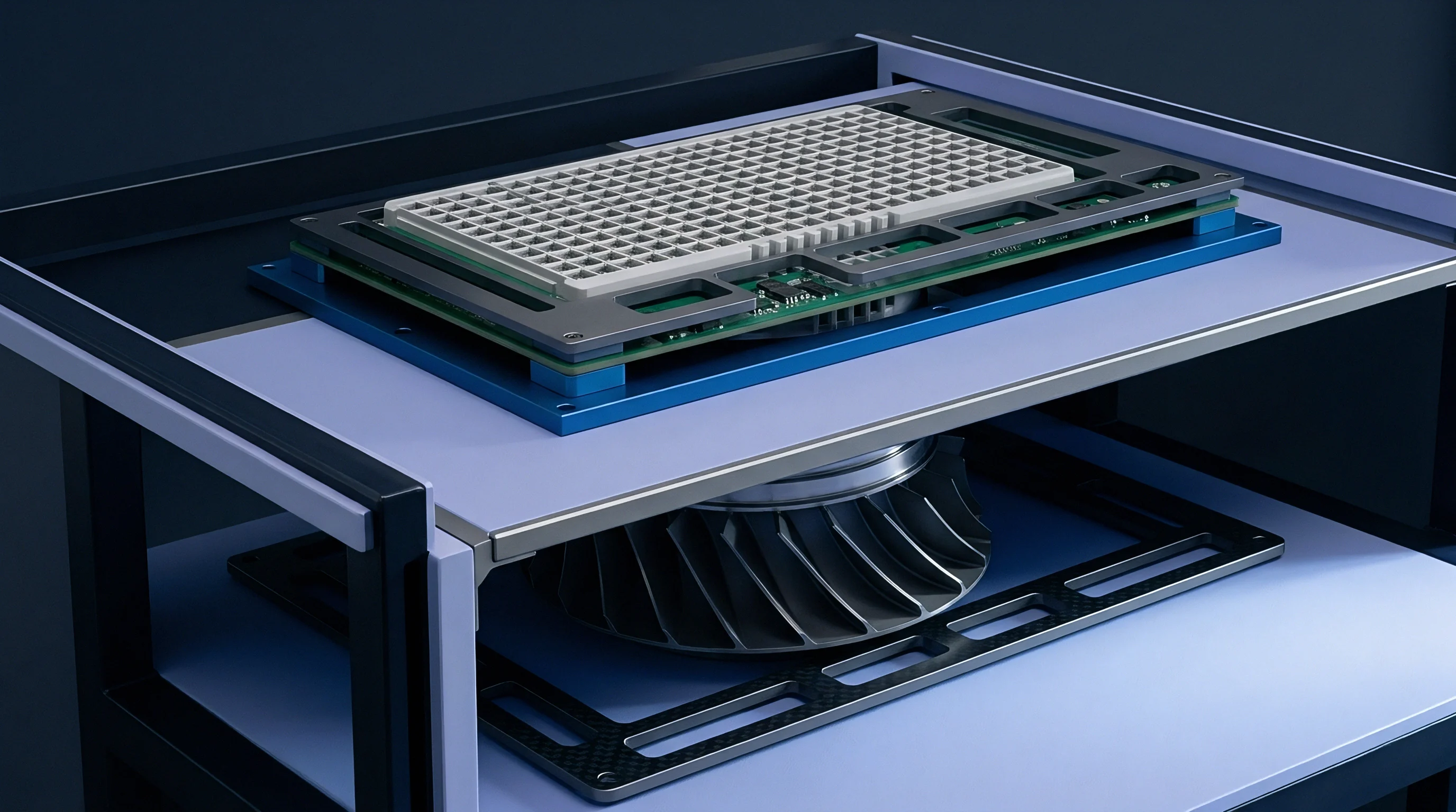
On-Chip OTP Trimming against Digital Register Offsets
Advanced sensor packages allow direct end-of-line programming of internal OTP memory banks to lock in post-reflow offset corrections. Applying a high-voltage programming pulse to dedicated IC pins burns micro-fuses within the digital logic die, permanently altering the default hardware offset register contents. On-chip OTP programming shifts the zero-point baseline permanently at the hardware level, relieving host firmware of executing offset subtraction logic on every boot cycle.
Programming OTP memory post-reflow demands strict control over programming voltages and ambient temperatures. Standard OTP fuse burning requires VPP programming voltages between 7.5 V and 12.0 V supplied with voltage regulation tolerances within plus or minus 2 percent. Applying out-of-spec programming pulses risks damaging adjacent digital logic or blowing partial fuses that revert state during long-term field operation.
A properly architected firmware architecture corrects for static mounting offsets without overwriting factory non-volatile temperature compensation coefficients.


Verification
Validating package stability and zero-point offset stability post-reflow requires rigorous laboratory testing profiles and acceptance sampling. Reliability protocols define specific environmental dwell periods, thermal shock profiles, and baseline drift limits to distinguish temporary post-assembly viscoelastic relaxation from permanent structural damage. IPC/JEDEC standards provide the foundational test profiles for verifying surface-mount sensor package robustness.
Quantifying post-reflow baseline movement demands high-precision laboratory test benches. Continuous data acquisition systems log sensor output voltages inside environmental test chambers held at constant temperature and humidity. Test setups isolate environmental variables, ensuring that observed register drift originates entirely from package strain relaxation rather than ambient thermal fluctuations.

Post-Assembly Thermal Dwell and Stabilization Envelopes
Stabilization envelopes define the mandatory waiting period between reflow soldering operations and final electrical test acceptance. Standard quality procedures enforce a minimum room-temperature dwell time before executing zero-point validation measurements. Immediate testing without an adequate dwell window yields inaccurate pass/fail classifications due to ongoing polymer stress relaxation.
IPC-TM-650 Method 2.4.43 deflection testing of QFN MEMS accelerometer packages indicates a 72-hour room-temperature dwell period for strain relaxation. Exceeding a glass transition temperature Tg of 150 °C during peak reflow extends this required relaxation window to 144 hours. Accelerated stabilization can be achieved by subjecting assembled boards to a low-temperature post-bake routine at 60 °C for 8 hours.
Low-temperature baking accelerates molecular relaxation within the mold compound without exceeding thermal stress limits.
- Symmetrical Thermal Relief Layout Implement four-spoke thermal relief patterns on all ground and power copper pads to balance heat transfer rates during reflow.
- Keep-Out Zone Implementation Maintain a minimum 3.0 mm exclusion zone around sensitive sensor footprints, barring large copper fills or structural mounting screws.
- Substrate Cutout Slots Routing mechanical isolation slots into the PCB surrounding three sides of the package footprint reduces board flexure strain transmission by up to 70 percent.
- Uniform Solder Paste Stencil Apertures Utilize electro-polished square stencil apertures with rounded corners to ensure identical solder volume deposition across all perimeter pads.

Acceptance Limits for Zero-Point Baseline Migration
Statistical quality control sets strict upper and lower acceptance thresholds for post-reflow offset drift. Zero-point shift distributions following standard reflow operations typically follow Gaussian profiles centered near zero millivolts, with spread defined by standard deviation values. Engineering specifications define upper control limits (UCL) and lower control limits (LCL) based on downstream application error budgets.
When batch offset distributions exhibit standard deviation expansion beyond 3 sigma limits, assembly process engineers investigate reflow profile symmetry, stencil alignment, and board warpage. Batches exceeding maximum drift limits undergo 100 percent recalibration or scrap disposition. Incorporating IPC-A-610 Class 3 co-planarity tolerances into the purchase order forces assembly partners to scrap boards exhibiting excessive local thermomechanical bowing.


Valuation
Package selection determines both the physical resilience of a sensor IC and its total landed integration cost. Component buyers evaluate multiple packaging options for a single sensor die design, ranging from unencapsulated bare-die wafer-level chip-scale packages (WLCSP) to fully molded QFN and ceramic cavity packages. Each package format presents distinct trade-offs between unit purchase price, printed circuit board assembly yields, post-reflow calibration costs, and long-term zero-point drift stability.
Wafer-level chip-scale packages provide the lowest upfront unit cost and smallest footprint area. WLCSP devices couple PCB thermal expansion stress directly into the silicon substrate. The absence of a protective plastic mold compound or copper leadframe leaves the active silicon exposed to direct solder joint shear strain.
High-precision applications using WLCSP sensors frequently incur secondary calibration expenditures that negate initial component savings, as factory trim adds twenty cents and board re-baking consumes twelve hours.
| Package Type | Unit Cost at 50k MOQ (USD) | Post-Reflow Offset Drift Typ (mV) | Factory Calibration Status | Board Space (mm²) | Total Landed Integration Cost (USD) |
|---|---|---|---|---|---|
| WLCSP (Bare Die with Bump) | 0.45 | ±4.50 | Wafer-Level Trim Only | 1.44 | 1.25 |
| Standard Plastic LGA (Plastic Molded) | 0.72 | ±1.80 | Fully Trimmed | 4.00 | 1.10 |
| Pre-Conditioned QFN (Exposed Pad) | 0.95 | ±0.60 | Fully Trimmed + Stress Relief | 9.00 | 1.18 |
| Hermetic Ceramic Cavity Package | 3.80 | ±0.10 | High-Precision Laser Trim | 25.00 | 4.25 |

Cost Balance between Factory Trim and Board Recalibration
Integrating zero-point recalibration steps into high-volume surface-mount manufacturing lines incurs direct operational expense. Running an automated zero-point calibration routine at final board functional test adds 1.5 to 4.0 seconds of cycle time per board. On high-volume automated lines producing 500,000 units annually, an extra 3.0 seconds of test time per unit consumes over 416 hours of line capacity, translating to substantial labor, capital depreciation, and energy overhead.
Buying pre-conditioned, stress-relieved sensor packages reduces downstream calibration requirements. Manufacturers subject pre-conditioned packages to thermal cycling and high-temperature storage prior to factory trimming, burning out initial viscoelastic relaxation drift. Pre-conditioned components command a 20 to 35 percent premium on unit purchase price.
This initial component cost increase is frequently offset by eliminating board-level oven baking and automated test-bench calibration cycles.

Delivered Unit Arithmetic across Package Formats
Total landed cost calculations compare component purchase price against all downstream manufacturing impacts. Consider a high-volume product requiring 100,000 sensors per year. Option A uses a low-cost plastic LGA sensor priced at $0.60 per unit.
Option B uses a high-stability pre-conditioned QFN sensor priced at $0.90 per unit. Option A exhibits a 3.5 percent post-reflow offset failure rate requiring manual board rework and secondary zero-point programming costing $4.50 per failed assembly. Option B exhibits a failure rate of 0.2 percent due to superior thermal gradient tolerance.
Option A incurs $60,000 in upfront component costs plus $15,750 in rework and calibration expense, yielding a total landed expenditure of $75,750. Option B incurs $90,000 in upfront component costs and $900 in rework expense, totaling $90,900. When board-level rework capacity is constrained, Option A wins purely on landed expenditure; however, if application specs mandate a zero-drift envelope below 0.5 mV, Option A fails field accuracy audits entirely.
Long-term drift figures post-reflow beyond 1,000 thermal cycles remain unquantified across low-cost plastic LGA packaging options due to sparse vendor aging datasets. The buyer addresses this uncertainty by inserting a mandatory 100-hour room-temperature stabilization burn-in clause into the component supply agreement prior to lot release.
Calculating total cost of ownership across volume manufacturing proves that paying a premium for pre-conditioned molded packages yields lower net expenditure than managing board-level zero-point calibration routines.