Thermal Processing
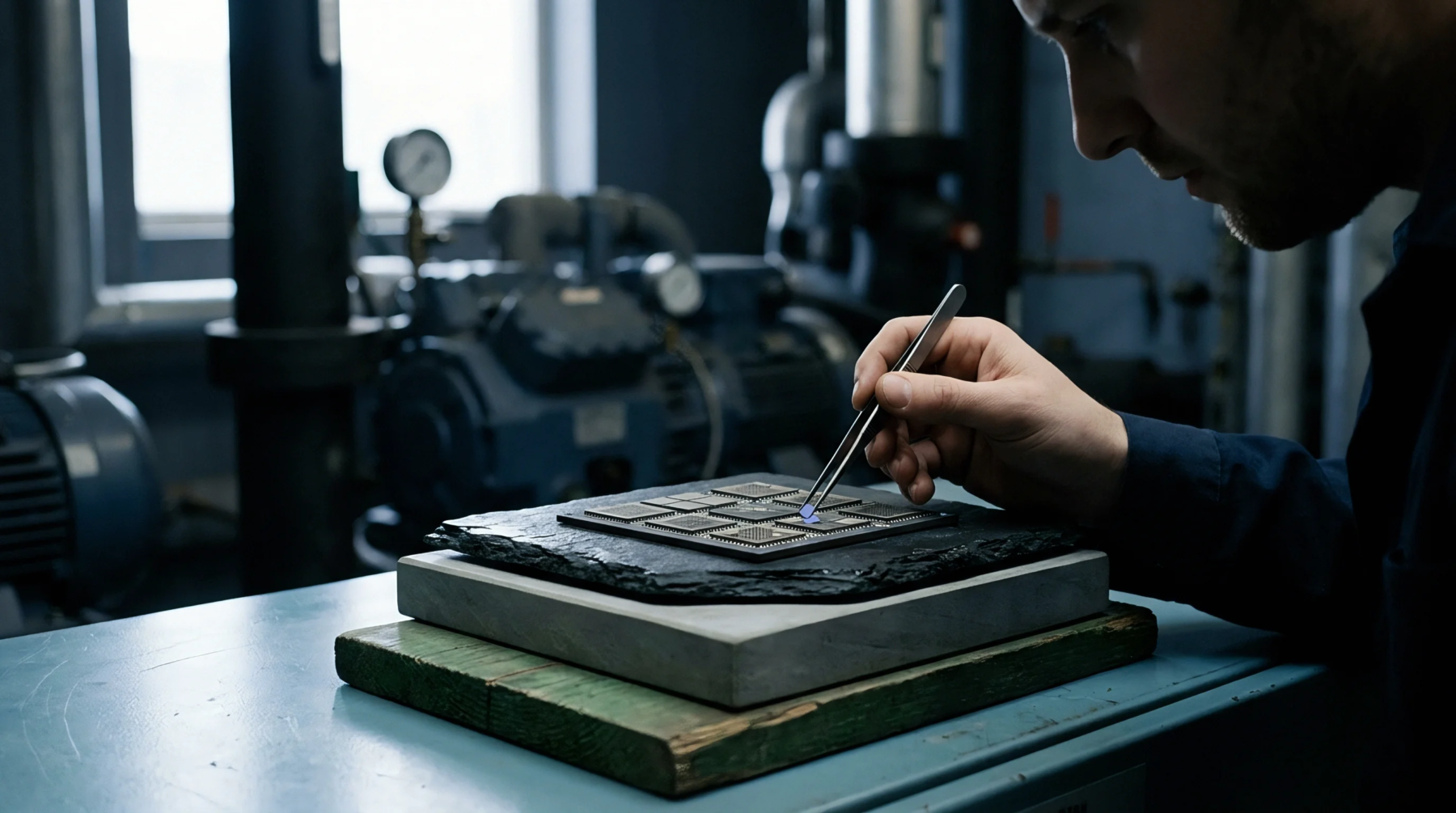
Controlled conveyorized heating chambers melt solder paste to form mechanical and electrical bonds between surface mount components and circuit board pads. Preheating, flux activation, liquidus melting, and controlled cooling stages execute sequentially in automated reflow ovens. The surface mount reflow process consolidates multi-component printed circuit assemblies in a single automated pass.
Physical bounds stop at liquidus temperature limits where component dielectric materials or package structures decompose.
Temperature Profile
Multi-zone forced convection ovens establish precise thermal profiles tailored to board mass and component sensitivity. Soak zones activate flux chemistries to remove surface oxides and reduce substrate thermal gradients prior to solder melting. Spike zones rapidly raise peak temperatures above liquidus values to ensure complete wetting of component terminals and copper pads.
Time above liquidus governs intermetallic compound growth thickness at solder interfaces. Rapid cooling rates yield fine grain microstructures with elevated mechanical strength, whereas excessively fast cooling risks thermal shock cracking in ceramic chip components.
Metallurgical Bonding
Molten solder alloys dissolve pad surface finishes to form intermetallic compound layers like Cu6Sn5 and Ni3Sn4. Controlled intermetallic layer growth creates metallurgical bonds between lead terminals and copper pads. Insufficient heat yields cold solder joints with poor wetting, while excessive heat degrades substrate epoxy resins.
Nitrogen inert gas atmospheres minimize oxidation during peak thermal exposure.
Process Limit
Maximum peak temperature limits protect heat-sensitive IC packages from delamination or internal wire bond damage. Solder balling defects occur when rapid ramp rates cause flux spattering. Surface mount reflow defines primary soldering parameters in microelectronics manufacturing.