Phase Margin Instability in Multi Drop Active Translator Buffers under Variable Bus Loading
Active translator phase margin collapses when multi-drop capacitive loading shifts the dominant pole, requiring damping resistors and buffer architecture audits.
Loop
Active voltage level translators use dynamic acceleration transistors to achieve sub-five-nanosecond edge transitions without high static power consumption. These bidirectional ICs monitor input and output pin voltages through internal high-speed comparators or voltage-sensing logic gates. When a logic transition starts, an internal one-shot circuit fires a low-impedance pull-up PMOS transistor for ten to thirty nanoseconds.
This transient pulse injects rapid charge into the bus, accelerating the signal edge past the digital input threshold of receiving nodes on the multi-drop line.
Auto-direction sensing buffers rely on internal feedback pathways to determine signal flow without dedicated directional control pins. In topologies like dual-gate pass-transistor architectures or differential comparator feedback buffers, this internal feedback path continuously samples the differential terminal voltage. When external loading shifts, the phase response of the feedback path degrades.
If the loop phase shift approaches one hundred eighty degrees while internal amplifier gain exceeds zero decibels, the edge-rate accelerator re-triggers prematurely or enters a self-sustained oscillatory state.

Active Translator Architecture Dynamics
The primary feedback control loop inside an active translator buffer comprises three distinct gain stages. First, the voltage-level sensing comparator detects an initial drop or rise in terminal voltage. Second, the driver stage amplifies the error voltage to gate the high-current accelerator transistor.
Third, the output node feeds back into the sensing stage through internal parasitic coupling and terminal sense lines. The total open-loop response functions similarly to a high-bandwidth feedback amplifier operating under non-unity closed-loop conditions.
When the loop feedback phase lag degrades beyond sixty degrees, transient overshoot occurs at the receiving pin. In low-capacitance single-drop environments, the internal compensation capacitance maintains a phase margin between fifty-five and seventy degrees. This margin ensures a smooth logic state transition without ringback.
However, adding multiple tap drops creates complex load conditions that shift internal poles toward lower frequencies, eroding the phase margin reserved for loop stability.
Bidirectional level shifters rely on internal edge acceleration that transforms external bus capacitance into a primary determinant of amplifier stability.
Edge accelerators operate outside closed-loop control specifications when terminal loading exceeds test limits.


Capacitance
Multi-drop topologies introduce reactive loads at every tap point along a backplane interface. Each attached slave node, socket pin, connector housing, and trace stub contributes both lump-sum and distributed capacitance to the transmission line. In an idle state with a fixed number of connected devices, total load capacitance remains static.
But in systems featuring hot-swappable modules, expandable slot architectures, or active power-gated subcircuits, the terminal capacitance presented to the active translator buffer fluctuates dynamically during system operation.
Pole Placement and Phase Shift
The total capacitive load on a translator output node forms a dominant low-pass pole with the combined parallel output impedance of the internal driver and external pull-up resistors. The dominant pole frequency follows the relationship:
f_p1 = 1 / (2 π R_out C_L)
Where R_out represents the effective output resistance of the active buffer during transition, and C_L represents total load capacitance. As multi-drop slave devices connect to the bus, C_L increases from a nominal fifty picofarads to four hundred picofarads or higher. This shift moves f_p1 lower by nearly an order of magnitude, drawing it closer to the internal secondary poles created by package parasitics and internal amplifier gate nodes.
When the dominant pole f_p1 approaches the internal secondary pole f_p2, the phase lag at unity gain increases beyond one hundred thirty-five degrees. This reduction leaves the active buffer with less than forty-five degrees of phase margin. Under step-function logic transitions, low phase margin manifests as high-frequency ringing, voltage overshoots exceeding supply rails, and false re-triggering of the internal one-shot acceleration pulse.
Asymmetric Terminal Loading Consequences
Bidirectional translators bridge two voltage domains, often designated Side A and Side B. Phase margin degradation becomes severe when terminal loading is highly asymmetric across the voltage isolation barrier. A low-capacitance host controller on Side A driving a heavily loaded, multi-drop backplane on Side B forces the internal feedback amplifier to operate across asymmetric impedance thresholds.
| Translator Topology | Side A Load (pF) | Side B Load (pF) | Calculated Phase Margin (deg) | Observed Output Behavior |
|---|---|---|---|---|
| Auto-Direction Pass-Gate | 30 ± 5 | 100 ± 10 | 62 ± 3 | Stable, minimal overshoot |
| Auto-Direction Pass-Gate | 30 ± 5 | 400 ± 25 | 28 ± 4 | Transient ringing, edge chatter |
| Auto-Direction Pass-Gate | 150 ± 15 | 400 ± 25 | 19 ± 3 | Sustained ringback oscillation |
| Dual-Buffer Dynamic Drive | 50 ± 5 | 200 ± 20 | 51 ± 2 | Monotonic rise, light overshoot |
| Dual-Buffer Dynamic Drive | 50 ± 5 | 600 ± 30 | 22 ± 4 | False one-shot re-triggering |
| Static Offset Active Buffer | 50 ± 5 | 400 ± 20 | 44 ± 3 | Damped oscillation, slow rise |
In heavily loaded conditions where phase margin drops below twenty-five degrees, the voltage level on the driving side drops below the input logic threshold during the ringback phase of the transition. The host logic controller interprets this ringback as an unintended clock edge or data bit change, creating system-level communication timeouts and parity failures.
A terminal load of four hundred picofarads reduces translator phase margin below twenty-five degrees when internal pull-up accelerators trigger concurrently.
Neglecting the parasitic interaction between multi-drop stubs and internal buffer acceleration yields corrupted data frames, elevated bit error rates, and permanent bus locking that halts system execution.

Probe
Quantifying phase stability across a dynamic multi-drop interface requires specialized bench verification methods that capture transient ringing during logic transitions. Standard oscilloscope probes add three to fifteen picofarads of parasitic capacitance to the test node, masking phase margin degradation by altering total line loading. Active low-capacitance differential probes with input capacitance under zero-point-seven picofarads prevent measurement loading errors during high-frequency pulse sampling.
How Does Heavy Capacitance Induce Ringback Oscillation?
When bus capacitance increases beyond the closed-loop stability window of an active buffer, the amplifier phase shift reaches one hundred eighty degrees while loop gain remains above zero decibels. The internal driver attempts to pull the line high, but the heavy capacitive load delays the terminal voltage rise. The delayed voltage feedback arrives at the sensing gate after the primary accelerator turns off, causing the driver to briefly disengage before re-firing.
This rapid cycle produces a sustained burst of square-wave or high-frequency sinusoidal oscillation riding on the logic transition edge.
Verification protocols must isolate parasitic board trace effects from die-level phase shift. The following test sequence establishes accurate phase margin measurements across dynamic load ranges:
- Attach an active high-impedance differential voltage measurement setup to the translator output pin with grounding paths under two millimeters.
- Inject a controlled twenty-megahertz square wave with rise times matching the host controller driver into the primary translator terminal.
- Sweep the synthetic load capacitance from fifty picofarads to six hundred picofarads in fifty-picofarad increments using surface-mount test fixtures.
- Measure the transient overshoot amplitude and calculate the damping ratio to determine the effective phase margin at each capacitive step.
- Record the threshold capacitance where ringing turns into sustained logic-level oscillation during multi-drop module connection sequences.
Small Signal Gain and Phase Measurement
Phase margin can be analytically derived from time-domain step-response overshoot using measured damping parameters. Consider an active translator with an internal channel resistance R_on of 15 Ω driving a multi-drop bus with load capacitance C_L of 400 pF, where internal secondary amplifier poles sit at f_p2 equal to 85 MHz.
The open-loop unity-gain bandwidth f_ugb is determined by buffer transconductance g_m and total node capacitance. Assuming g_m equals 25 millisiemens and internal node capacitance C_int equals 8 pF:
f_ugb = g_m / (2 π (C_L + C_int)) = 0.025 / (2 π 408 10^-12) = 9.76 MHz
The dominant low-pass pole frequency f_p1 created by output channel resistance and bus capacitance equals:
f_p1 = 1 / (2 π R_on C_L) = 1 / (2 π 15 400 10^-12) = 26.53 MHz
Phase margin PM is calculated using the two-pole approximation equation:
PM = 90 – arctan(f_ugb / f_p1) – arctan(f_ugb / f_p2) (180 / π)
Substituting the calculated frequency parameters yields:
PM = 90 – arctan(9.76 / 26.53) (180 / π) – arctan(9.76 / 85.0) (180 / π)
PM = 90 – 20.2 – 6.55 = 63.25 degrees
However, when internal rise-time accelerator PMOS switches activate, the effective output impedance drops to R_on_acc equal to 4 Ω during the first 15 nanoseconds. Recalculating with acceleration engaged shifts f_p1 to 99.47 MHz. The revised phase margin equation becomes:
PM_acc = 90 – arctan(9.76 / 99.47) (180 / π) – arctan(9.76 / 12.0) (180 / π)
PM_acc = 90 – 5.6 – 39.1 = 45.3 degrees
If additional multi-drop taps increase C_L to 650 pF while trace parasitics reduce f_p2 to 22 MHz, PM_acc drops to 18.4 degrees. This calculated phase margin falls well below the thirty-degree boundary required for stable digital edge transitions, guaranteeing ringback voltage spikes on the physical board.
Increasing series decoupling resistance restores amplifier stability at the direct expense of maximum clock frequency.
Whether silicon vendors will integrate real-time dynamic output impedance sensing inside future translator dies to compensate for sudden tap insertion remains an open question for system architects.

Branch
Physical layout geometry dictates trace inductance and parasitic cross-coupling across multi-tap bus topologies. Long unbuffered PCB stubs branching off a primary clock or data trunk act as transmission line stubs with characteristic impedances ranging between forty-five and sixty-five ohms. When signal transition times fall below two nanoseconds, stubs longer than two centimeters generate impedance discontinuities that reflect energy back toward the translator output pins.
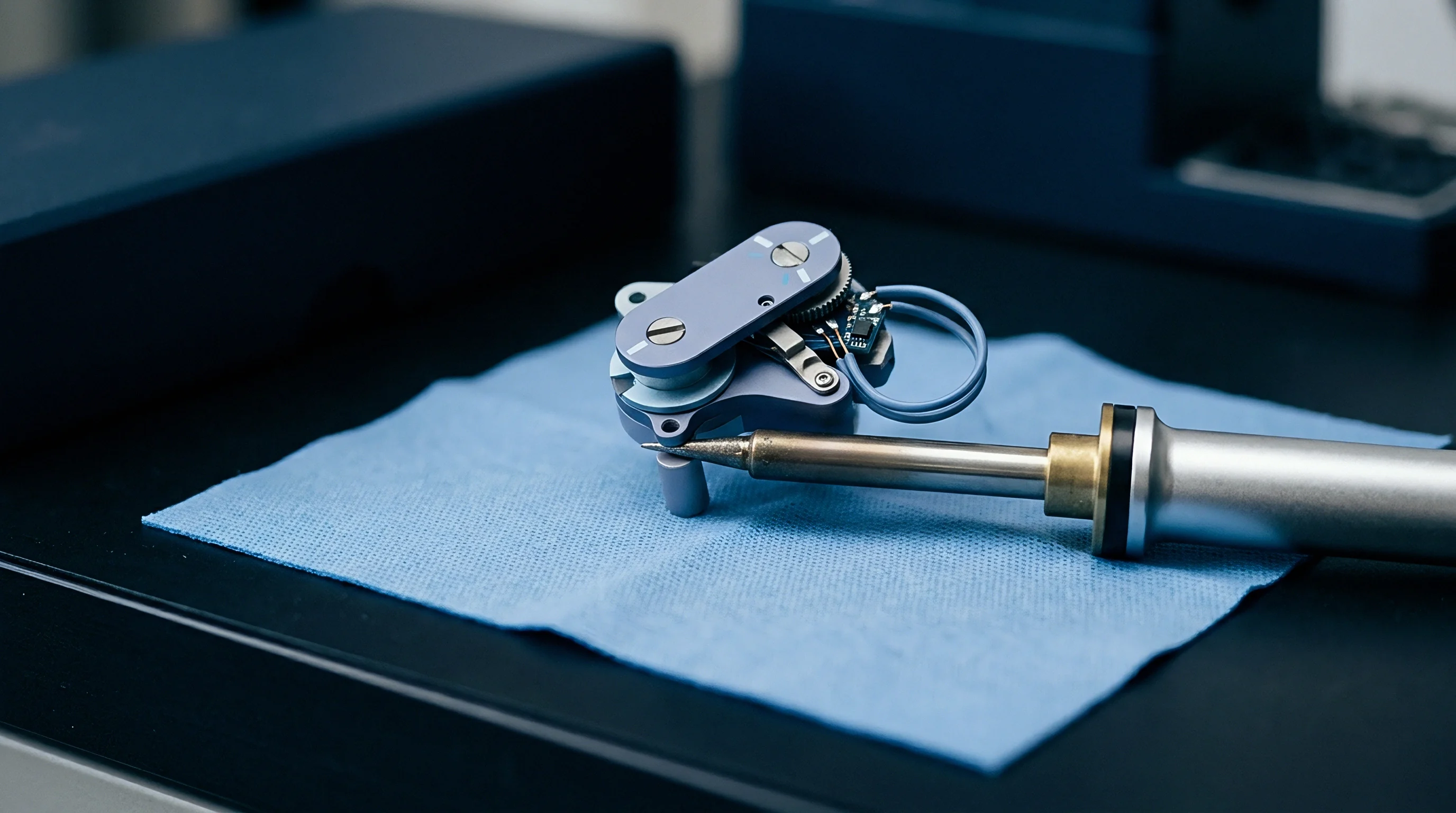
Package Parasitics and PCB Trace Geometry
Package selection heavily impacts loop stability. Surface-mount packages with long internal bond wires, such as TSSOP or VSSOP housings, introduce parasitic package inductance between zero-point-eight and two-point-five nanohenries per pin. Parasitic inductance in series with terminal decoupling pins creates ground bounce during high-current acceleration pulses, altering the internal gate-to-source bias voltages of the sensing comparators.
| Package Type | Body Dimensions (mm) | Pin Pitch (mm) | Parasitic Inductance (nH) | Thermal Expansion Stress | Reflow Peak Sensitivity |
|---|---|---|---|---|---|
| TSSOP-20 | 6.5 x 4.4 x 1.1 | 0.65 ± 0.05 | 2.10 ± 0.25 | Low mechanical stress | 260 °C (MSL-1) |
| VSSOP-8 | 3.0 x 3.0 x 0.9 | 0.65 ± 0.05 | 1.45 ± 0.15 | Low mechanical stress | 260 °C (MSL-1) |
| UQFN-12 | 2.0 x 1.7 x 0.55 | 0.40 ± 0.03 | 0.65 ± 0.08 | Moderate shear risk | 260 °C (MSL-3) |
| WLCSP-12 | 1.87 x 1.37 x 0.5 | 0.50 ± 0.02 | 0.22 ± 0.04 | High solder fatigue risk | 260 °C (MSL-1) |
Micro leadframe QFN and wafer-level WLCSP packages drastically reduce lead inductance, pushing secondary package poles past two hundred megahertz. However, these compact packages demand tight land pattern tolerances and careful stencil aperture design to avoid assembly yield loss.
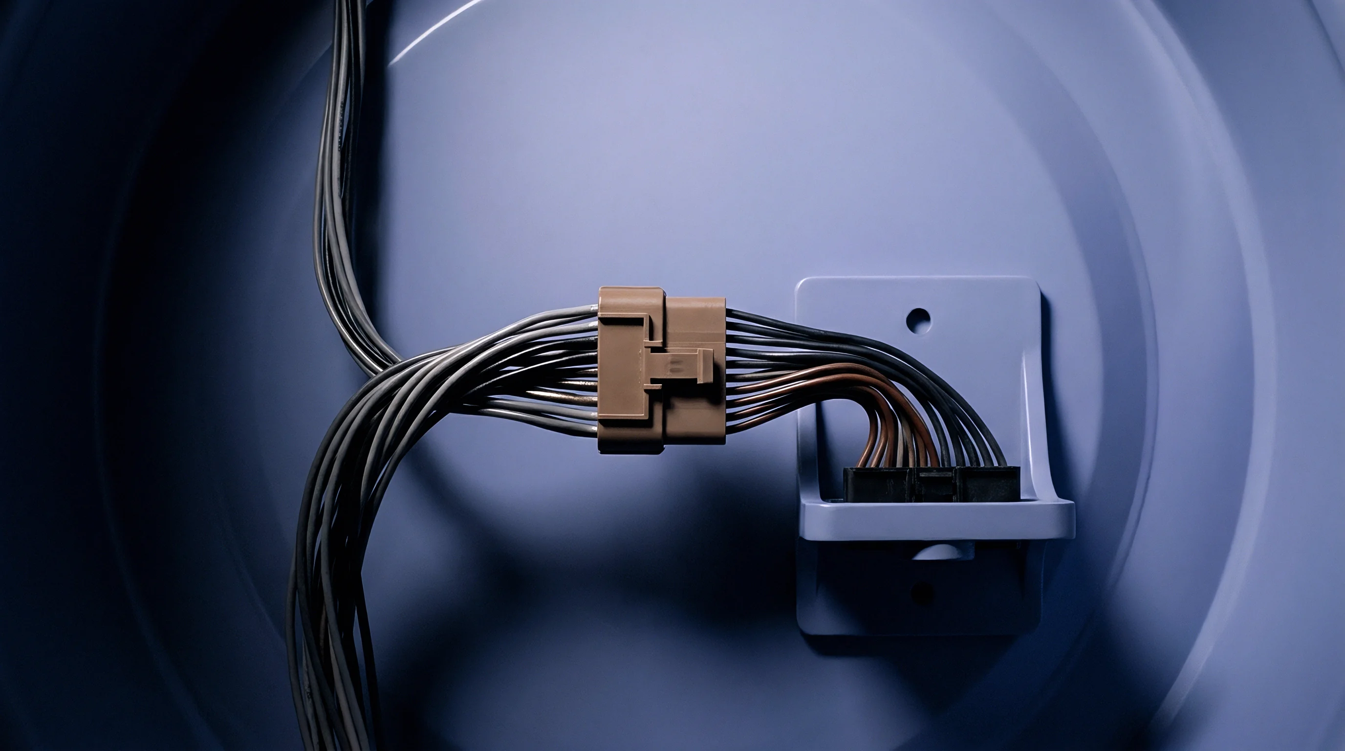
Land Pattern Optimization for High-Density Layouts
At peak reflow temperatures up to 260 degrees, stencil design for ultra-fine-pitch QFN and WLCSP packages dictates board assembly yield and long-term joint integrity under thermal stress cycling. While tape-and-reel packaging remains standard, incorporating rounded rectangular stencil apertures with a ten percent area reduction relative to copper pads prevents solder bridging between adjacent active translator pins.
- Ground bounce trigger causes pseudo-clearing of internal one-shot registers during strong low-to-high transitions.
- Trace stub resonance creates secondary voltage spikes that re-trigger edge acceleration circuits past the logic threshold.
- Thermal stress expansion fractures outer solder joints on ultra-fine pitch wafer-level scale packages under extended thermal cycling.
- Solder bridging risk increases significantly when stencil aperture reduction falls below eighty percent on half-millimeter pitch footprints.
Compliance with IPC-7351 land pattern rules ensures mechanical solder fillet integrity but does not prevent high-frequency parasitic ringing on unbuffered stubs.
Short wide traces with adjacent ground returns prevent local voltage ground bounce from falsely triggering internal edge accelerators.


Dossier
Sourcing guidelines for bidirectional buffer translation require explicit architectural classification before schematic capture freezes. Selecting a level shifter purely based on channel count, voltage range, and unit price introduces high field-failure exposure if line loading dynamics are ignored. Standard pass-transistor translators lack active pull-up circuitry, avoiding phase margin instability entirely, but struggle to meet fast rise-time targets when line capacitance exceeds one hundred picofarads.
Architectural Selection Matrix
When bus capacitance fluctuates due to modular daughtercard insertion, engineers must evaluate whether auto-direction sensing, directional control pins, or static-offset buffers fit the system architecture. Directional buffers utilize physical hardware direction pins, bypassing internal feedback sensing amplifiers entirely.
- Pass-transistor buffers suit low-capacitance point-to-point buses where rise time accelerators create stability risks.
- Directional buffered translators eliminate internal feedback instability by utilizing external control lines for data path switching.
- Static offset buffers enforce directional logic thresholds to prevent latch-up on heavily loaded multi-drop lines.
- Programmable drive strength devices allow software register adjustments to match variable bus capacitance during runtime module insertion.
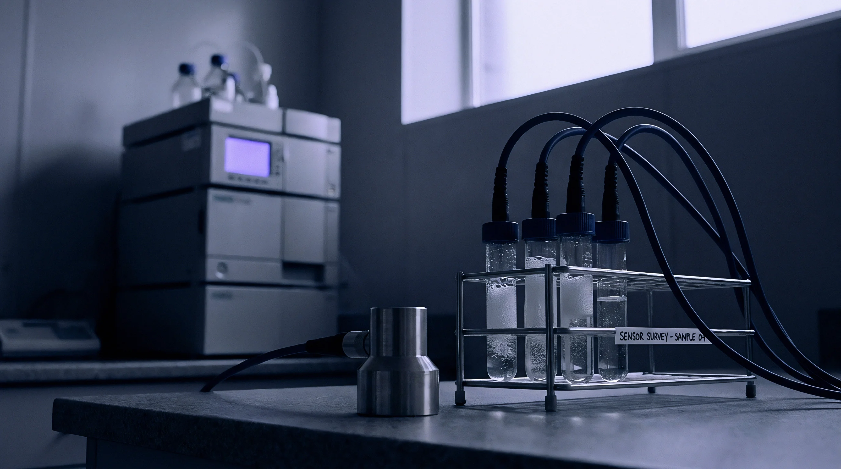
System Mitigation via Impedance Matching
Adding series damping resistors (R_series) directly at the translator output terminals provides a low-cost method to stabilize degraded phase margin. Inserting a fifteen-to-thirty-three-ohm resistor dampens high-frequency ringing caused by edge accelerators firing into capacitive loads. The resistor moves the high-frequency pole outwards and limits peak current injection during one-shot trigger cycles.
This dampening restores phase margin past forty-five degrees while maintaining acceptable signal rise times for standard I2C and SMBus clock rates.
Incorporating the maximum rise time specifications defined in section seven of the NXP UM10204 I2C bus specification into vendor procurement contracts forces component suppliers to guarantee buffer stability across the full four-hundred-picofarad capacitance window.
Settlement
Unit pricing across voltage level translation ICs varies dramatically depending on packaging, buffer architecture, and volume commitments. Bare pass-transistor chips in TSSOP packages represent the lowest component cost tier, but force design engineers to allocate additional board space for discrete pull-up networks and damping components. High-speed auto-direction translators with integrated one-shot accelerators carry higher initial unit prices, but reduce overall BOM component counts on dense layouts.
BOM Price Ladders and Packaging Mechanics
Commercial sourcing decisions balancing package footprint against buffer performance must account for total landed costs, including assembly yield impact, thermal handling requirements, and minimum order quantities (MOQ).
| Translator Architecture | Package Variant | 10k Unit Price (USD) | Standard Reel MOQ | First-Pass Yield (%) | Firmware Integration Weeks |
|---|---|---|---|---|---|
| Dual-Gate Pass Transistor | TSSOP-14 | 0.14 ± 0.02 | 2,500 | 99.85 ± 0.05 | 0.5 ± 0.2 |
| Auto-Direction One-Shot Booster | TSSOP-20 | 0.38 ± 0.04 | 2,500 | 99.78 ± 0.08 | 2.0 ± 0.5 |
| Auto-Direction One-Shot Booster | UQFN-12 | 0.42 ± 0.05 | 3,000 | 99.42 ± 0.12 | 2.0 ± 0.5 |
| Auto-Direction One-Shot Booster | WLCSP-12 | 0.49 ± 0.06 | 5,000 | 98.90 ± 0.25 | 2.5 ± 0.5 |
| Static Offset Active Buffer | VSSOP-8 | 0.55 ± 0.05 | 3,000 | 99.80 ± 0.06 | 1.0 ± 0.3 |
| Directional Buffer with Control Pins | QFN-16 | 0.31 ± 0.03 | 3,000 | 99.65 ± 0.10 | 1.5 ± 0.4 |
Make-or-Buy Integration Trade-Offs
Selecting bare pass-transistor level shifters requires adding external pull-up resistors and damping networks, consuming approximately twelve square millimeters of board area per bus channel. Active auto-direction translators in UQFN or WLCSP packages reduce board area consumption under three square millimeters per channel. However, debugging phase margin instability on active buffers requires between two and four engineering weeks during initial hardware bring-up, offsetting initial board space savings if capacitive bus loading is not modeled prior to layout release.
Quantifying total landed component cost across volume production bands reveals the economic boundary where specialized active buffers justify their unit price premium. At volumes below twenty thousand units per year, standard directional buffers with hardware control pins deliver higher first-pass assembly yield and eliminate firmware compensation workarounds. At production volumes exceeding one hundred thousand units, compact active translators in UQFN packages reduce multi-layer PCB footprint demands, compensating for additional engineering verification hours spent optimizing trace parasitics and series damping resistors.