Silicon Resonator Frequency Drift under Uniform Thermal Loading
Degenerate boron doping and electrostatic tuning compensate silicon resonator thermal frequency drift within five parts per million across broad thermal spans.
Drift
Single-crystal silicon resonators shift operational frequency under uniform thermal excitation primarily through the temperature dependence of their elastic constants. For a double-clamped beam or a clamped-free cantilever, the fundamental resonant frequency depends on geometric dimensions and equivalent material stiffness, scaling with the square root of Young’s modulus divided by mass density. Thermal expansion alters length, width, and thickness at roughly 2.6 parts per million per Kelvin at room temperature, but this dimensional change is secondary to the drop in elastic modulus.
The temperature coefficient of Young’s modulus in both isotropic and anisotropic silicon outweighs dimensional expansion by more than an order of magnitude. For an uncompensated, pure single-crystal silicon resonator operating in flexural, longitudinal, or higher modes, the first-order temperature coefficient of frequency falls between negative thirty and negative thirty-five parts per million per Kelvin near 298 Kelvin. As substrate temperature climbs uniformly, structural stiffness drops, slowing the resonator at a rate set by the elastic properties along the chosen crystallographic direction, such as the 100 or 110 orientation.
Single-crystal silicon exhibits a uncompensated temperature coefficient of frequency of negative thirty-one parts per million per Kelvin at two hundred ninety-eight Kelvin.
Thermal loading acts on acoustic velocity directly. Rayleigh waves, Lamé modes, and bulk acoustic waves all track the temperature dependence of stiffness tensor components, specifically c11, c12, and c44. The temperature coefficient of c44 sits at negative sixty parts per million per Kelvin, while c11 reaches near negative seventy-five parts per million per Kelvin.
When a package experiences a uniform thermal step, heat conducts through the substrate, die attach, and anchors, bringing the resonant element to isothermal equilibrium within milliseconds. Across an industrial range of negative forty degrees Celsius to eighty-five degrees Celsius, uncompensated drift runs almost linearly before second-order thermal coefficients introduce quadratic curvature at higher temperatures.
In narrow-band synthesis and precision timing circuits, this uncompensated linear drift quickly degrades performance. Several common failure modes appear under uniform ambient thermal swings:
- Clock skew in synchronous buses accumulates phase error between distributed nodes when local thermal dissipation elevates ambient die temperature above baseline calibration limits.
- Channel crosstalk in RF transceivers occurs when local oscillator drift shifts transmission carriers into adjacent frequency channels during environmental temperature transitions.
- Sensor drift in resonant transducers corrupts strain or pressure measurements by confounding thermally induced frequency changes with mechanical force inputs.
- Phase-locked loop unlocked states trigger when resonator frequency shifts exceed the pullability range or capture bandwidth of active tuning circuits.
Overlooking the first-order temperature coefficient during initial component selection routinely causes calibration failures during thermal qualification. If a board layout ignores that native negative thirty parts per million per Kelvin shift, fixing it later demands external temperature-compensated crystal oscillators or digital calibration routines that eat up unplanned PCB area and power.
Doping
Heavy carrier concentration in single-crystal silicon alters the electronic contribution to free energy, shifting the temperature derivative of elastic stiffness. Concentrated boron or degenerate phosphorus doping alters electron-phonon coupling across the crystal lattice. Once p-type concentration passes 10 to the 19th power atoms per cubic centimeter, the temperature coefficient of the shear elastic constant c44 actually changes sign from negative to positive over target temperature intervals.
Passive compensation balances this electronic softening against composite material structures. Thermal silicon dioxide has a positive temperature coefficient of Young’s modulus, around positive eighty-five parts per million per Kelvin. Growing or depositing a thin oxide layer onto the outer surfaces of a silicon beam offsets the negative coefficient of the bulk core, yielding a net zero first-order temperature coefficient of frequency at a chosen turnover temperature.
However, thermal expansion mismatch between the amorphous oxide shell and the crystalline core leaves residual strain at the interface during thermal cycling.
Heavy degenerate p-type doping inverts the temperature coefficient of Young’s modulus while increasing acoustic loss within the resonant beam.
Compensating resonators through material alteration inevitably introduces trade-offs. The heavy doping that corrects the thermal coefficient also introduces energy dissipation paths that degrade the mechanical quality factor, elevating the phase noise floor and forcing sustain circuits to burn more drive power. Similarly, composite oxide-silicon beams show thermal hysteresis under wide thermal excursions as strain relaxes along the amorphous-crystalline boundary.
Selecting passive compensation methods for high-stability MEMS resonators involves several structural boundaries:
- Degenerate p-type doping concentration achieves zero first-order temperature coefficient of frequency when boron concentration reaches 2.5 times 10 to the 19th power atoms per cubic centimeter along specific crystallographic axes.
- Thermal oxide cladding ratio requires precise oxide-to-silicon thickness ratios, typically near 1 to 10 for flexural modes, to align the zero-TCF turnover point with room temperature.
- Crystallographic orientation selection aligns flexural or shear motion along the 100 direction to maximize the compensation efficiency of degenerate doping profiles.
- Annealing cycle control removes interface traps and relieves micro-strains between oxide layers and silicon substrates to minimize frequency hysteresis during repeated thermal cycles.
Batch-to-batch frequency drift discrepancies are tracked both to oxide deposition thickness variations and to unacknowledged dopant activation gradients across six-inch production wafers. When incoming inspection logs a three parts per million per Kelvin variance across wafer lots, the underlying cause tends to sit between atmospheric pressure shifts during oxidation cycles and non-uniform carrier activation.
Furnace
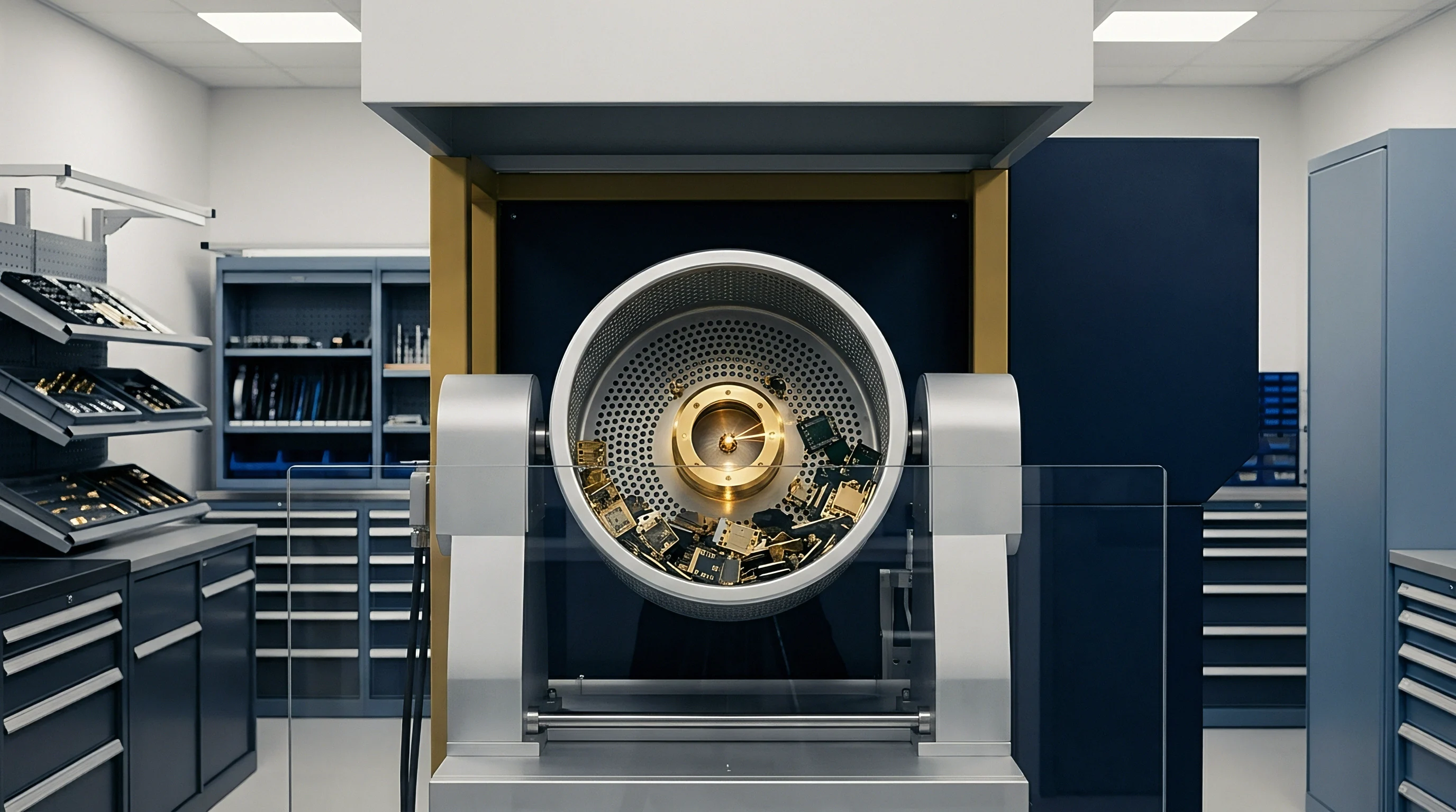
Testing in an environmental chamber isolates intrinsic resonator behavior by eliminating spatial thermal gradients. When a packaged MEMS resonator sits in a steady furnace, heat conducts through the leadframe, solder joints, die pad, and anchors until the resonant beam matches the surrounding air. The tiny thermal mass of micro-scale resonators allows internal temperatures to equalize within microseconds.
Within a hermetically sealed cavity, heat transfer is governed almost entirely by anchor conduction; radiative transfer across sub-micron gaps is negligible below 125 degrees Celsius.
Ovenized MEMS resonators integrate micro-heaters directly onto the silicon die to hold the structure at a set temperature above the maximum expected ambient. Micro-machined isolation bridges etched into the bulk substrate provide high thermal resistance between the heated resonator island and the package floor. By holding this local micro-oven at the turnover temperature, frequency drift stays under one part per million across ambient swings from negative forty degrees Celsius to eighty-five degrees Celsius.
IEC 60068-2-14 specifies thermal equilibrium verification when frequency rate of change drops below one hundredth of a part per million per minute.
Where Does Thermal Resistance Limit OCXO Power Budgets?
Maximizing thermal resistance cuts the heater power needed to sustain internal operating temperatures, but it concentrates mechanical stress at the anchor points. The table below lists physical properties governing thermal and elastic performance for key microelectronic resonator materials under uniform thermal loads at 298 Kelvin.
| Material Phase | Density (kg/m³) | Thermal Conductivity (W/m·K) | Expansion Coefficient (ppm/K) | First-Order TCF (ppm/K) |
|---|---|---|---|---|
| Single-Crystal Silicon <100> | 2330 | 148 | 2.6 | -31.0 |
| Thermal Silicon Dioxide (SiO₂) | 2200 | 1.4 | 0.5 | +85.0 |
| Polycrystalline Silicon | 2320 | 30 | 2.8 | -34.0 |
| Polycrystalline Germanium | 5323 | 60 | 5.8 | -65.0 |
| Boron-Doped Silicon (2.5e19 cm⁻³) | 2330 | 95 | 2.6 | +2.5 |
Separating package stress relaxation from true material drift requires a rigorous bench routine. Chamber verification typically proceeds through four steps:
- Mount the packaged resonator under test into a low-stress socket positioned in the center of the thermal chamber workspace.
- Connect low-capacitance RF cabling to a frequency counter referenced to a rubidium atomic standard.
- Ramp chamber temperature at one degree Celsius per minute to target soak temperatures from negative forty to one hundred twenty-five degrees Celsius.
- Dwell at each ten-degree increment for thirty minutes to ensure complete die thermalization before logging resonant frequency data.
Whether thermal stress at silicon anchor boundaries introduces non-recoverable physical displacement after multiple thermal cycles remains an open topic in high-reliability automotive qualification research.

Silicon
Electromechanical tuning exploits electrostatic softening to counteract changes in elastic modulus across operating temperatures. Applying a direct current bias across capacitive drive or sense gaps alters the beam’s net spring constant, which equals the raw mechanical stiffness minus an electrostatic term proportional to the bias voltage squared divided by the cube of the gap width. By steering the bias voltage through a dedicated temperature sensor and digital-to-analog converter, active feedback can null both first- and second-order temperature coefficients of frequency.
Consider a flexural silicon MEMS resonator operating at a baseline frequency of 10 MHz at 298 Kelvin with an uncompensated temperature coefficient of negative thirty parts per million per Kelvin. Under uniform heating to 348 Kelvin, representing a 50 Kelvin thermal load step, the resonant frequency drops without compensation by 1500 Hz, settling at 9.9985 MHz. To pull the frequency back to 10.0000 MHz electrostatically, the closed-loop controller reduces the DC bias voltage across a 100-nanometer capacitive gap, reducing electrostatic softening and restoring total structural stiffness.
Electrostatic stiffness tuning corrects residual thermal drift at the cost of elevated phase noise floor.
Active compensation architectures trade stability directly against circuit power, phase noise, and die area. Wide tuning authority requires narrow gaps or substantial voltages, both of which introduce non-linearities into the signal path. The matrix below summarizes practical boundaries across common mitigation schemes.
| Compensation Type | Frequency Stability (ppm) | Power Consumption | Phase Noise Impact | Die Area Overhead |
|---|---|---|---|---|
| Uncompensated Bulk Silicon | ±1500 (-40 to +85°C) | Zero | Baseline Best | None |
| Passive Dopant / Oxide Layers | ±30 (-40 to +85°C) | Zero | Moderate Q Loss | Low |
| Analog Electrostatic Tuning | ±5 (-40 to +85°C) | < 50 microwatts | Elevated Near-In | Medium |
| Digital Fractional-N Synthesis | ±0.5 (-40 to +85°C) | 1 to 5 milliwatts | Spurious Tones | High |
| Micro-Ovenized Die (OCXO) | ±0.1 (-40 to +105°C) | 20 to 100 milliwatts | Low | Very High |
Feedback topology dictates how well an active thermal compensation circuit performs in practice. Core implementation rules include:
- Temperature sensor integration proximity demands placing on-chip diode or resistor thermal sensors within fifty micrometers of resonator anchors to minimize thermal response delay.
- Resolution of tuning digital-to-analog converters mandates sixteen-bit minimum resolution to prevent discrete frequency jumping during gradual ambient temperature ramps.
- Bias voltage supply rejection ratio requires low-dropout regulators with sub-microvolt noise density to avoid converting supply ripple into phase jitter via electrostatic tuning interfaces.
- Look-up table memory calibration density requires multi-point polynomial fit parameters stored in non-volatile memory across at least five distinct temperature calibration points.
Designing aggressively for low drift without monitoring loop phase noise merely trades one problem for another, shifting the system bottleneck from frequency accuracy to jitter in high-speed clocks.

Market
Commercial sourcing of silicon oscillators hinges on wafer-level vacuum packaging yields and thermal hysteresis inside transfer-molded plastic. Bare MEMS resonators need high-vacuum cavities to achieve quality factors above 100,000, typically using gold-silicon eutectic bonds or glass-frit seals to prevent viscous air damping. Once packaged, thermal expansion mismatches between epoxy molding compound, copper leadframes, and the silicon die translate external thermal changes into mechanical stress.
Manufacturing economics heavily favor passive compensation over per-unit trimming. Cycling individual parts through temperature chambers inside automated test handlers multiplies dwell times, pushing test and calibration costs from cents into dollars. As a result, high-volume consumer gear relies on oxide layers or moderate doping to hold stability within plus or minus 10 to 20 parts per million across industrial temperatures.
Telecom and automotive infrastructure choose digitally compensated or micro-ovenized devices instead, trading unit cost and higher current draw for sub-part-per-million accuracy over operating life.
Automotive standards AEC-Q100 Grade 1 and AEC-Q103 place tight limits on post-cycling drift between negative forty degrees Celsius and one hundred twenty-five degrees Celsius. Parts must prove their frequency offsets remain within published datasheet limits across 1000 thermal shock cycles. Failures during stress testing often trace back to moisture ingress in the mold compound, which sets up uneven strain fields across the wafer-level cap.
Supply contracts for industrial timing devices tie drift thresholds directly to environmental testing schedules. Standard procurement language defines the overall frequency budget: The component shall maintain a total frequency tolerance within plus or minus 10 parts per million across all operational conditions, including initial frequency tolerance at 25 degrees Celsius, thermal drift over the temperature range from negative forty degrees Celsius to eighty-five degrees Celsius, supply voltage variations of plus or minus five percent, and 10-year aging effects under continuous thermal exposure.