Managing Electrical Parasitics and Capacitance in Extended Bus Sensor Harnesses
Managing sensor harness parasitics demands fluoropolymer dielectrics, matched line termination, active buffer acceleration, and strict shield grounding topology.

Trunk
Taking digital or precision analog sensor lines off the circuit board brings distributed electrical properties into play that change signal behavior. A cable harness acts like a distributed complex network rather than a clean zero-resistance trace. Copper conductors add loop resistance, adjacent pairs introduce distributed capacitance, and physical wire geometry creates loop inductance along the run.
Driving a fast digital edge or reading a high-impedance analog sensor through an extended harness introduces low-pass filtering, propagation delays, and resonant voltage spikes.
These electrical parameters stem directly from conductor dimensions and dielectric insulation properties. Resistance depends on American Wire Gauge, stranding, and copper purity. Shunt capacitance between conductors is largely set by the dielectric constant of the insulating polymer, wire outer diameter, and center-to-center spacing.
Stray inductance comes from the loop area between the signal path and its return. In long runs, ignoring these parasitics leads to corrupted data, dropped frames, and offset errors in analog signals.
Physical Conductor Geometry and Distributed Line Parameters
Longer runs increase total series resistance and parallel capacitance proportionally. Resistance per unit length goes up as wire diameter shrinks: standard 28 AWG wire has a DC loop resistance of about 0.21 ohms per meter, while heavier 22 AWG measures roughly 0.053 ohms per meter. When sensor nodes draw power or switch current through thin wires, series resistance creates DC voltage drops that shift local ground relative to the host controller.
How conductors are arranged inside the jacket sets mutual inductance and capacitance. Parallel pairs give higher mutual capacitance per meter than widely separated single wires. Twisting conductors into balanced pairs keeps wire spacing uniform, stabilizing differential impedance and minimizing loop area.
Parallel pair inductance scales with the logarithm of the ratio of center-to-center distance to conductor radius. Squeezing wires closer together slightly reduces inductance but sharply increases mutual capacitance.
Distributed inductance along the harness resists fast current changes. Standard unshielded twisted pair cables have self-inductance values between 0.5 and 0.8 microhenries per meter. Rapid digital transitions on high-inductance runs produce inductive voltage spikes when current stops suddenly ~ such as when a driver drops into a high-impedance state.
Managing these parameters requires checking cable specs well before choosing connector hardware.
Dielectric Constant Impact on Shunt Capacitance
Insulation material sets the baseline shunt capacitance of the cable assembly. Permittivity indicates how much energy a material stores in an electrostatic field relative to a vacuum. Standard polyvinyl chloride has a high dielectric constant between 3.0 and 4.0, resulting in high capacitance between conductors.
Polyethylene, fluorinated ethylene propylene, and expanded polytetrafluoroethylene have lower constants between 2.0 and 2.3, reducing signal energy storage.
Shunt capacitance loads down open-drain and push-pull drivers alike. Typical PVC-insulated signal cable has mutual capacitance between adjacent wires of 90 to 130 picofarads per meter. Switching to fluorinated ethylene propylene drops that to 40 to 55 picofarads per meter for the same gauge and spacing.
On a twenty-meter run, choosing a low-dielectric polymer eliminates over fifteen hundred picofarads of parasitic capacitance.
This capacitive load charges and discharges on every bit transition. Higher shunt capacitance forces signal drivers to supply more current to change states, creating dynamic current spikes on edge transitions. These transients flow back through ground, introducing high-frequency noise into sensitive analog circuits on the same power rail.
| Insulation Polymer Type | Dielectric Constant | Shunt Capacitance (pF/m) | Loop Resistance 24 AWG (Ω/m) | Nominal Impedance (Ω) |
|---|---|---|---|---|
| Polyvinyl Chloride | 3.4 | 115 | 0.084 | 75 |
| Semi-Rigid Polyvinyl Chloride | 3.0 | 98 | 0.084 | 85 |
| High-Density Polyethylene | 2.3 | 58 | 0.084 | 100 |
| Fluorinated Ethylene Propylene | 2.1 | 46 | 0.084 | 120 |
| Expanded Polytetrafluoroethylene | 1.7 | 34 | 0.084 | 135 |
Environmental exposure changes dielectric performance over time. PVC absorbs moisture in humid environments, increasing its dielectric constant and raising parasitic capacitance. Fluoropolymer insulations absorb almost no moisture, holding mutual capacitance steady as ambient humidity changes.
Temperature also shifts polymer permittivity, causing baseline capacitive loading to drift in hot industrial or automotive installations.
Fluoropolymer insulations hold shunt capacitance below fifty picofarads per meter while standard vinyl jackets exceed double that value.
Physical construction also affects effective dielectric permittivity. Cables using micro-cellular air-foamed insulation achieve low capacitance because air has a dielectric constant near 1.0. Adding an overall foil shield around a pair increases capacitance to ground, since the metallic shield acts as another conductive plane near the signal wires.
Designing for specific transmission specs requires balancing shield distance against wire spacing.
Selecting conductor gauge requires balancing electrical performance against cable flexibility and weight. Heavier wire lowers series resistance and DC drop, but makes the harness thicker, stiffer, and heavier. Stranded conductors handle continuous vibration better than solid wire, though spiraled strands slightly increase DC resistance due to longer effective path lengths.
Shielded cables with thin fluoropolymer walls keep outer diameters small while maintaining low capacitance over long runs.
As a simple rule of thumb, use the lowest permittivity insulation available whenever harness length exceeds three meters.

Reflectance
Signal transition speed determines whether a harness acts as a simple capacitive load or a distributed transmission line. If the driver’s signal rise time is shorter than twice the electrical delay down the cable, high-frequency edge components treat the harness as a continuous transmission channel. Under these conditions, physical variations or impedance mismatches cause signal reflections to bounce back and forth along the line.
Propagation velocity in copper wire depends on the relative permittivity of the insulation. Electromagnetic waves travel through copper in standard fluoropolymer dielectrics at roughly sixty-eight to seventy-five percent of the speed of light in a vacuum. That translates to a delay of about 4.5 to 4.9 nanoseconds per meter.
A ten-meter run introduces a one-way delay around 47 nanoseconds, creating a round-trip reflection time of nearly 94 nanoseconds.

Transmission Line Limits in Extended Digital Bus Topology
Fast digital output transitions excite high-frequency harmonic modes in long cables. If a microcontroller output pin has a 2-nanosecond rise time, any harness longer than about twenty centimeters behaves as a transmission line. Open-drain buses like Standard Mode I2C use slower rise times set by pull-up resistors, but push-pull SPI, UART, and single-ended clock lines create sharp edges that trigger severe reflections over distance.
Impedance mismatches at cable ends reflect signal energy back toward the driver. An open-circuit termination at an unbuffered sensor reflects the incident edge with identical amplitude and polarity. The reflection combines with the incoming wave, creating a voltage overshoot that can exceed the receiver IC’s maximum voltage rating.
The wave then travels back to the transmitter, where a low driver output impedance reflects it again with inverted polarity, causing damped ringing.
Ringing on clock and data lines causes false triggers in edge-sensitive input stages. If ringing crosses the logic threshold multiple times during a single transition, microcontrollers register extra clock pulses, corrupting register transfers and forcing bus resets. Parasitic inductance in connector pins and board traces sharpens these reflection artifacts, worsening overshoot and undershoot.

Impedance Mismatch Mechanics and Edge Degradation
Mismatch severity depends on the difference between driver output impedance, cable characteristic impedance, and receiver input impedance. Standard unshielded twisted pair runs at 100 to 120 ohms characteristic impedance, while custom multi-core sensor cables can drop to 50 ohms or rise above 150 ohms. CMOS push-pull drivers typically present low output impedances of 10 to 40 ohms, while receiver inputs present over 10 megohms in parallel with a few picofarads of pin capacitance.
Preventing reflections requires matching strategies suited to the bus topology. Series termination places a resistor at the driver pin so the combined driver and resistor impedance matches the cable’s characteristic impedance. This absorbs reflections returning from the receiver without adding static DC current draw.
Parallel termination places a resistor equal to characteristic impedance across the far end of the bus, absorbing signal energy completely, though it continuously draws DC power when the signal is held low.
Stubs along a multi-drop sensor harness create local impedance discontinuities that trigger secondary reflections. When drop cables connect the main trunk to individual nodes, each stub acts as an unterminated branch. Signals on the main line split at the junction, reflect off the open stub end, and re-enter the trunk delayed in time.
To preserve signal integrity, stub lengths should stay under one-tenth of the electrical transition length of the fastest edge.
- Impedance Discontinuity Ringing causes false clock edge detection when reflected waves cross input logic thresholds repeatedly during a single bit period.
- Voltage Overshoot Transients force ESD protection diodes inside receiver chips into forward conduction, introducing high substrate current spikes.
- Signal Undershoot Inversion drives input pins below local ground potential, triggering parasitic latch-up conditions in sensitive CMOS integrated circuits.
- Phase Jitter Accumulation shifts digital sampling points away from the center of data bit cells, raising bit error rates on extended UART runs.
Calculated series termination values must account for manufacturing variations in trace and wire dimensions. Driver impedance also shifts with temperature and supply voltage, requiring tolerance-stackup analysis. If driver output impedance drops at low temperatures, series damping becomes less effective, allowing larger reflections to persist on the line.
Driver drive strength must be evaluated against total harness impedance to prevent severe signal degradation before laying out interface hardware. Installing damping resistors near transmitter output pins absorbs edge energy that would otherwise disrupt receivers down the line. High-speed signals running over multi-meter cables require termination placed as close as possible to the physical connector pins.
Standard unshielded copper harnesses are often treated as reliable up to ten meters without termination, but fast driver transition times degrade signal margins regardless of cable length.


Attenuation
Signal amplitude drops along a harness as DC resistance and AC capacitive loading consume available drive current. On extended digital buses, attenuation appears as reduced logic high levels, elevated logic low levels, and degraded rise times. Open-drain sensor interfaces are especially vulnerable to capacitive loading because logic high transitions rely entirely on passive pull-up resistors to charge bus capacitance.
Total bus capacitance includes transmitter and receiver pin capacitance, PCB trace capacitance, connector parasitics, and the distributed shunt capacitance of the cable. Standard open-drain buses like I2C specify maximum allowable capacitance to ensure transitions complete within timing windows. Standard Mode (100 kilobits per second) and Fast Mode (400 kilobits per second) I2C both cap total bus capacitance at 400 picofarads.

Rise Time Constraints and Active Current Injection
Choosing passive pull-up values requires trading off rise time against driver current sinking. Charging a capacitive bus through a fixed resistor produces an exponential curve set by the RC time constant. The rise time from 30% to 70% of supply voltage equals 0.8473 times pull-up resistance times total capacitance.
Lower resistance speeds up charging but increases DC power draw and forces drivers to sink more current when holding the line low.
When total harness capacitance exceeds 500 picofarads, passive pull-ups cannot meet fast rise time targets without exceeding driver sinking limits. Standard I2C drivers sink a maximum of 3 milliamps while keeping low-level output voltage below 0.4 volts. On a 3.3-volt supply, minimum passive pull-up resistance is 1.1 kilohms.
At this limit, a harness with 2 nanofarads of distributed capacitance yields an RC rise time over two microseconds ~ violating standard timing limits and stalling the bus.
Active pull-up circuits overcome rise time limits by swapping static resistors for dynamic current injection. Active bus accelerators monitor line voltage during low-to-high transitions. When voltage crosses a lower threshold, internal transistors turn on, injecting a high-current pulse to rapidly charge distributed harness capacitance.
Once voltage reaches an upper threshold, the accelerator turns off, returning to a high-impedance state so the line holds its logic high level cleanly.
Consider a fifteen-meter sensor network using multi-core PVC-insulated cable. Distributed mutual capacitance between data and ground is 110 picofarads per meter, giving 1650 picofarads of cable capacitance. Input capacitance from ten sensor modules adds 70 picofarads, bringing total bus capacitance to 1720 picofarads.
The calculation below shows the limits of passive charging versus dynamic current acceleration for this setup:
Under passive pull-up operation using the minimum allowable 1.1 kilohm resistor, the calculated 10% to 90% rise time is:
Rise Time = 2.2 x R x C = 2.2 x 1100 ohms x 1.72 x 10^-9 farads = 4.16 microseconds.
This 4.16-microsecond transition exceeds the maximum allowed Standard Mode I2C rise time of 1.0 microsecond by more than 400 percent. Running this bus requires dropping clock frequency below 20 kilobits per second or replacing passive pull-ups with an active accelerator IC capable of supplying 10 milliamps of transition current during edges.

DC Drop and Logic Threshold Compression
DC resistance in long harnesses shifts ground and power supply potentials at remote sensor nodes. When multiple sensors draw current at the same time, voltage drop across thin ground wires raises local ground potential relative to the host controller. This offset reduces noise margins for single-ended logic.
Logic low thresholds limit how much ground offset can be tolerated. For standard 3.3-volt CMOS logic, maximum input low voltage is 30% of supply (0.99 volts), while transmitter output low voltage is guaranteed at or below 0.4 volts. That leaves a static low-state noise margin of 0.59 volts.
If ground loop currents or power return drops cause a 0.4-volt shift across ground, the available noise margin drops to 0.19 volts, making the interface vulnerable to EMI spikes.
| Drive Architecture | Max Bus Capacitance (pF) | Max Harness Distance (m) | Dynamic Power Dissipation | Relative System Cost |
|---|---|---|---|---|
| Standard Passive Pull-Up | 400 | 3 | Low (Static DC Sinking) | Base Level |
| Switched Active Bus Accelerator | 4000 | 20 | Moderate (Transient Pulses) | 1.4x |
| Dual-Buffer Bidirectional Isolation | 3000 | 30 | Moderate (Continuous Drive) | 2.1x |
| Differential Bus Conversion (CAN/RS485) | 10000 | 1200 | High (Constant Differential) | 3.5x |
Distributing power at higher voltages helps offset DC line drop in distant sensor clusters. Main supplies can run at 12 or 24 volts down the cable, then step down using local LDOs or small buck converters at each sensor node. Local regulation stabilizes supply rails at transducer dies, keeping internal analog references steady despite line drops and changing load currents.
Analog sensor interfaces suffer severe DC attenuation when driving low-impedance receiver inputs over long wires. Transducer output impedance combines with harness resistance and receiver loading to form an uncompensated voltage divider. Current through parasitic loop resistance changes calibrated scale factors, requiring high-impedance differential buffers at the receiver end.
Maximum allowable I2C bus capacitance limits Standard Mode speed to four hundred picofarads under standard ten to ninety percent rise time windows.
Analog signal attenuation can also be eliminated by switching from voltage-mode signals to current loops. A standard 4-to-20 milliamp current loop drives a modulated current through conductors regardless of line resistance, up to the compliance limit of the transmitter. Within reasonable bounds, parasitic series resistance causes zero measurement error in a current loop, provided the transmitter has enough voltage compliance to handle the loop drop.
Specifying current-mode conversion ICs for analog sensor harnesses over five meters eliminates capacitive attenuation. Transmitting signals as currents bypasses high-frequency shunt loading and DC voltage drop errors. Local transconductance amplifiers convert transducer voltages into current signals right at the sensor package before entering the main cable.
Ignoring cumulative capacitance on long open-drain lines leads to intermittent data corruption, lost acknowledge bits, and bus lockups under thermal stress.

Interference
Long harnesses act as antennas, picking up external noise and coupling transient fields into nearby circuits. Running signal lines, power conductors, and high-current actuator wires inside the same jacket creates strong parasitic coupling paths. Managing these requires disciplined routing, targeted shielding, and proper ground handling.
Crosstalk between parallel conductors comes from mutual capacitive and inductive coupling. Capacitive crosstalk occurs when changing voltage on an active line induces transient current into an adjacent high-impedance line through parasitic capacitance. Inductive crosstalk occurs when switching currents generate local magnetic fields that induce noise voltages in adjacent loops inside the harness.

What Shield Grounding Topology Prevents Ground Loops?
Single-point shield grounding prevents low-frequency power currents from circulating through harness braids. Grounding a shield to chassis at both ends of a long run forces compensation currents through the braid whenever ground potentials differ between locations. This circulating ground loop current couples low-frequency hum and voltage noise onto internal signal wires through transfer impedance.
Single-ended shield grounding bonds metallic foil or braid to system ground at the host controller end while leaving the far end floating. This breaks ground loop paths entirely, providing strong protection against low-frequency electrostatic fields. At high frequencies where cable length approaches a fraction of a wavelength, however, single-point shields lose effectiveness due to standing waves on the ungrounded shield.
Hybrid shield grounding protects against both low-frequency ground loops and high-frequency noise. The shield braid connects directly to ground at the primary host end and connects to chassis ground through a low-inductance ceramic capacitor at the far end. This provides high DC impedance to block low-frequency ground loops while offering a low RF impedance path to ground high-frequency noise at both ends.
Drain wire termination at connector backshells directly affects transfer impedance. Pigtail connections formed by twisting braid strands into a thin wire add significant parasitic series inductance ~ up to 10 nanohenries per centimeter. At high frequencies, this inductance creates a high-impedance path to ground, degrading shielding performance and allowing coupled noise to radiate onto internal conductors.

Capacitive Coupling Mechanics in Multi Conductor Bundles
Mutual capacitive coupling strength scales with line length and switching edge speed. Coupled crosstalk voltage equals the ratio of mutual capacitance to total line capacitance, multiplied by the signal voltage step size on the active trace. Slowing active driver edge rates with low-pass filters or slew-rate-controlled drivers reduces high-frequency current injected into adjacent passive signal lines.
Differential signaling provides inherent rejection of common-mode capacitive and inductive noise. In balanced differential pairs like CAN, RS-485, or LVDS, noise couples into both conductors equally in phase and amplitude. Receiver stages measure the voltage difference between conductors, subtracting identical common-mode noise and preserving signal integrity over long runs in noisy environments.
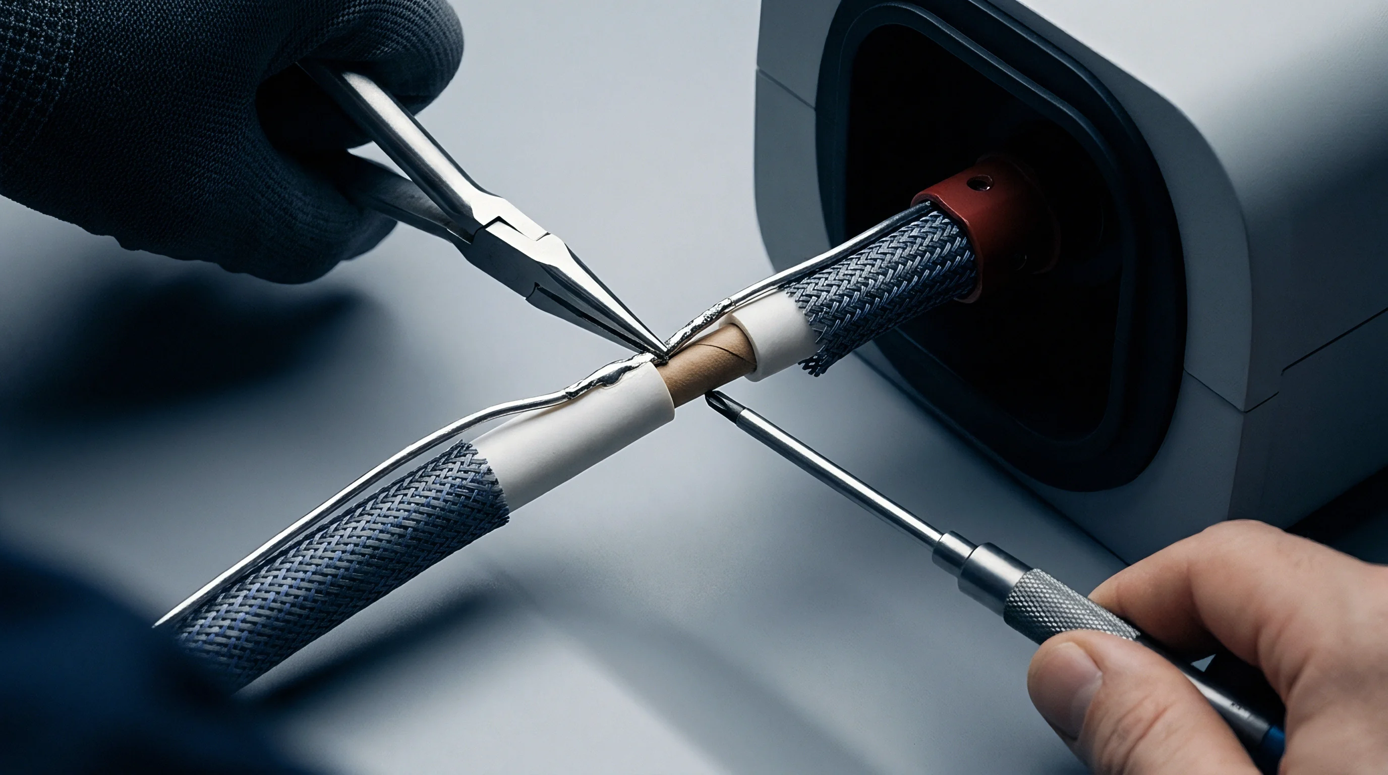
- Strip back outer cable jacket insulation without damaging metallic shield braid or inner conductor jacketing.
- Unbraid exposed shield strands smoothly and fold them backward over the outer perimeter of the connector clamping adapter.
- Position a 360-degree metallic compression ring over the folded shield strands to establish continuous circumferential ground contact.
- Thread clamping hardware tightly onto the connector housing to lock the shield assembly mechanically and electrically.
Star-quad wire arrangements further reduce inductive noise pickup in compact multi-conductor cables. Arranging four conductors as two diagonally opposing pairs inside a single jacket ensures both wires of a differential pair maintain the same average distance to external noise sources. This geometric symmetry balances noise coupling, providing high crosstalk rejection without extra insulation bulk.
Choosing unshielded multi-conductor cable to save on initial BOM costs creates persistent field vulnerabilities that require expensive software filtering and retransmission routines later. Differential lines combined with proper shield grounding preserve clean waveforms over long distances without complex error-correction code on the host.
Whether unshielded twisted pair cabling can maintain reliable digital telemetry in heavy motor noise depends on local field strength and driver edge rates.

Provisioning
Matching physical interface components to harness characteristics dictates system reliability and assembly costs. Standard microcontrollers have limited current drive and narrow voltage tolerance ranges that suit on-board traces, not external cables. Wiring raw silicon pins directly to multi-meter harnesses risks latch-up, severe edge degradation, and ESD damage in the field.
Physical layer buffer ICs bridge the gap between silicon drivers and long harness parasitics. Bidirectional bus buffers break capacitive loads into isolated physical segments, preventing total cable capacitance from accumulating on microcontroller trace nodes. Specialized heavy-duty driver ICs convert low-voltage single-ended logic into high-current or differential signals capable of driving long, capacitive wires without frame errors.

Physical Layer Buffer IC Selection and Driver Topologies
Selecting buffer components requires balancing dynamic current drive, package footprint, operating voltage, and unit cost. Simple open-drain accelerators offer economical edge charging for runs up to ten meters. Beyond ten meters, or in noisy environments, differential line transceivers deliver far better noise immunity and signal integrity at the cost of higher power draw and larger PCB area.
Level-shifting bus buffers like the PCA9600 allow single-ended open-drain signals to drive low-impedance, high-current lines. The chip splits standard logic into separate transmit and receive channels, allowing pull-up resistors on the cable side to be reduced to 82 ohms. Sinking up to 30 milliamps, these buffers can drive up to 4000 picofarads of harness capacitance, supporting Standard Mode bus communication over thirty meters of unshielded twisted pair.
Galvanic isolation ICs eliminate ground loops entirely while passing high-speed digital sensor data across long distances. Optocouplers, capacitive digital isolators, and magnetic isolation transformers isolate local host grounds from remote sensor chassis potentials up to several kilovolts. Installing isolated transceivers at harness endpoints protects host electronics from high-voltage surges, ground offsets, and continuous common-mode voltage differences in facility deployments.
| Transceiver IC Architecture | Max Data Rate | Capacitance Tolerance | Package Options | Unit Cost 1k Qty (USD) |
|---|---|---|---|---|
| Switched Active Accelerator | 1.0 Mbps | Up to 3000 pF | SOT-23, MSOP-8 | $0.85 |
| High-Current Logic Buffer | 1.0 Mbps | Up to 4000 pF | SOIC-8, TSSOP-8 | $1.45 |
| Isolated Differential Transceiver | 10 Mbps | Up to 10000 pF | SOIC-16 Wide Body | $3.80 |
| Precision Current-Loop Transmitter | 100 kHz | Unrestricted (Current) | QFN-16, SOIC-8 | $2.20 |

Analog Signal Conditioning for Extended Distance Transducers
Precision analog sensor signals require dedicated conditioning at the host receiver to overcome line resistance drops and high-frequency noise pickup. High-impedance operational amplifiers in instrumentation configurations provide high common-mode rejection, canceling noise coupled equally onto both leads of a long sensor cable. Placing low-pass RC filters directly at amplifier input terminals attenuates RF interference before it can undergo non-linear rectification in input transistor stages.
Active filtering at host receiver inputs must balance noise rejection against bandwidth. Setting filter cutoff frequencies too low introduces phase delay and settling lag in high-speed closed-loop control systems. Using low-drift, precision operational amplifiers with low input bias currents ensures high-impedance sensors operate accurately without baseline loading errors over long wire runs.
- Component Package Selection forces trade-offs between thermal dissipation capability, lead pitch inspection yield, and available board area in compact sensor housings.
- Thermal Resistance Limits restrict maximum drive current in small surface-mount package options operating under elevated ambient temperatures.
- Connector Pin Pitch Space dictates minimum trace spacing and restricts maximum voltage clearance distances between high-voltage surge paths.
- Automotive Qualification Levels dictate component sourcing options and increase landed unit costs for specialized extended-temperature integrated circuits.
Sourcing strategy must account for package form factor and driver software support before freezing schematic designs. Relying on single-sourced physical layer transceivers creates severe supply chain risk during component allocations. Standardizing on common SOIC and QFN footprints ensures secondary source availability without requiring board respins during volume production.
Standard JEDEC J-STD-020 reflow profiles require checking component moisture sensitivity levels before surface-mount assembly, preventing package popcorning during high-temperature reflow passes.


Audit
Verifying extended harness parasitics requires dedicated bench testing before system qualification. Standard digital multimeters only measure static DC resistance, missing high-frequency transmission behavior, distributed capacitance anomalies, and reflection issues. Proper harness qualification combines time-domain analysis, frequency-swept impedance testing, and margin verification under environmental stress.
Time Domain Reflectometry provides precise spatial resolution of impedance variations along a cable assembly. A reflectometer sends a fast voltage step with a rise time under 100 picoseconds down the harness and measures the timing and amplitude of reflected waves returning to the instrument. Analyzing these reflection signatures pinpoints pinched insulation, damaged shields, bad connector contacts, and local impedance shifts down to millimeter accuracy.

Time Domain Reflectometry and Harness Capacitance Profiling
Reflectometry traces give accurate quantitative measurements of characteristic impedance along the entire cable run. An upward reflection indicates an inductive discontinuity or high-impedance fault, such as a loose connector pin or broken wire strand. A downward pulse reveals a capacitive fault, like crushed insulation, shorted conductors, or moisture ingress inside the jacket.
Measuring propagation delay across a known cable length confirms the effective dielectric constant of the insulation.
LCR meters measure total shunt capacitance and loop inductance across frequency sweeps. Testing harnesses from 1 kilohertz to 10 megahertz exposes dielectric dissipation factors and frequency-dependent capacitance. Cables with high loss tangents at elevated frequencies convert fast signal edge energy into heat, attenuating digital harmonics and dulling edge transitions at receiver inputs.
Insulation resistance testing under high DC potential verifies dielectric breakdown margins between conductors. Applying up to 500 volts DC between signal wires and the surrounding shield confirms insulation integrity. Measured isolation resistance should exceed 500 megohms under dry conditions to keep micro-ampere leakage currents from shifting delicate analog calibrations.

Bench Margin Measurement and Acceptance Verification
Eye diagram analysis measures overall signal degradation on high-speed digital sensor buses. An oscilloscope samples incoming data triggered over repetitive clock cycles, overlaying successive bit transitions into a single composite view. The eye opening dimensions quantify timing jitter, noise margin, rise time performance, and inter-symbol interference caused by harness parasitics.
A clean, wide eye opening indicates healthy timing and voltage margins with low bit error probability. A collapsing eye signals severe signal degradation, warning that noise transients or temperature shifts will cause bit errors at receiver ICs. Measuring eye height and width across extreme operating temperatures sets hard length limits for specific cable and driver combinations.
Testing harness prototypes in environmental thermal chambers verifies dielectric stability across operating temperature limits. Measuring total shunt capacitance and signal edge timing at minus forty degrees Celsius and plus one hundred twenty-five degrees Celsius catches performance drift before releasing harness documentation for production. Documenting these bounds prevents raw cable lot variations from impacting field reliability.
Signal sweeps combined with time-domain reflectometry provide definitive pass/fail metrics for incoming harness qualification. Establishing clear electrical acceptance criteria in manufacturing procurement specs prevents substandard wiring assemblies from reaching production lines.