Dynamic Stability Analysis of Operational Amplifier Reference Buffers
Operational amplifier reference buffers driving heavy capacitive loads require isolation resistors or dual-feedback networks to prevent dynamic instability.

Trace
Placing a 10 µF multilayer ceramic capacitor directly on the output pin of a low-noise amplifier shifts the dominant open-loop pole to lower frequencies while introducing a secondary pole at the open-loop output resistance. High-precision analog-to-digital converters require continuous charge replenishment at their reference terminals during sample-and-hold transitions. When the driving buffer lacks sufficient phase margin, high-frequency current steps excite the resonant circuit formed by the board routing inductance and the decoupling capacitance.
Oscillations or prolonged ringing at the reference node corrupt the conversion results, generating differential non-linearity errors in high-resolution data acquisition systems.
Routing geometries on multi-layer printed circuit boards introduce parasitic physical parameters that alter loop stability. Copper tracks add roughly 0.8 nH of inductance per millimeter, along with distributed trace capacitance to adjacent ground planes. In high-bandwidth reference buffer designs, this parasitic inductance isolates the feedback network from the physical load capacitor at megahertz frequencies.
The phase shift accumulated across the physical routing combines with the internal phase lag of the silicon die, eroding the phase margin until the circuit reaches absolute instability.
Uncompensated open-loop output impedance transforms capacitive reference loads into high-Q resonant tanks.
Layout parasitics modify loop gain. Printed circuit board trace resistance and via inductance shift the location of closed-loop poles. When a designer places a decoupling array far from the buffer output pin, the interconnect inductance forms an uncontrolled L-C tank circuit with the low equivalent series resistance ceramic capacitors.
Small signal disturbances trigger sustained ringing at the output. Uncompensated networks ring prolonged.
Evaluating layout geometries requires checking the parasitic loop inductance against the open-loop output resistance of the operational amplifier die. Standard FR-4 dielectric substrates introduce capacitive coupling between adjacent signal layers, adding up to 1.2 pF per inch of parallel routing. This stray capacitance across the feedback resistor creates an unexpected feedback zero, altering the high-frequency attenuation slope.
If the open-loop output resistance remains high across frequency, the phase angle drops past negative 180 degrees before the loop gain crosses unity, causing self-sustained oscillation.
- Parasitic Trace Inductance increases the total loop phase shift by inserting an uncompensated high-frequency pole into the open-loop transfer function.
- Low Capacitor ESR eliminates the stabilizing zero normally contributed by legacy tantalum units, exacerbating phase margin loss across temperature extremes.
- Distributed Ground Impedance lifts the reference ground potential during transient load steps, introducing common-mode disturbance into the operational amplifier feedback path.
- Feedback Path Stray Capacitance bypasses the high-frequency isolation resistor, coupling load-side noise directly back into the inverting input terminal.
Ignoring trace parasitics during initial layout shifts closed-loop poles into the right half-plane, forcing an expensive printed circuit board spin and delaying product qualification by several months.

Damping
Feedback stability degrades rapidly when an operational amplifier drives a large capacitive reference decoupling array without isolation. The internal open-loop output resistance forms a low-frequency pole with the load capacitance. This pole reduces phase margin long before the loop gain drops to 0 dB.
Precision amplifiers often exhibit open-loop output resistance values between 20 Ω and 100 Ω. Driving a 10 µF load directly yields a pole located below 8 kHz, degrading loop stability in unity-gain configurations.

Feedback Loop Degradation in Large Capacitive Reference Architectures
A high open-loop output resistance combined with a 47 µF ceramic filter network creates a low-frequency pole that reduces loop phase margin below 15 degrees. Small signal gain peaking appears in the closed-loop frequency response, amplifying high-frequency noise. Excess phase triggers oscillation.
Phase margin falls rapidly. Loop stability collapses. Adding a small isolation resistor between the operational amplifier output pin and the load capacitor introduces a zero into the feedback transfer function, stabilizing the loop at the expense of DC load regulation.
| Topology Configuration | Output Resistance (Ω) | Load Capacitance (µF) | Phase Margin (Degrees) | Settling Time to 0.001% (µs) |
|---|---|---|---|---|
| 50 | 10 | 8.5 | 450.0 | |
| 50 | 10 | 58.0 | 12.5 | |
| 50 | 10 | 64.5 | 4.2 | |
| 50 | 10 | 52.0 | 18.0 |
The in-loop dual-feedback topology restores DC precision while maintaining stability across heavy capacitive loads. High-frequency feedback passes through a small capacitor directly from the operational amplifier output pin, bypassing the load isolation resistor. Low-frequency feedback connects after the isolation resistor, sensing the true DC reference voltage at the load capacitor.
This split-path feedback decouples high-frequency phase shift from the primary feedback loop, retaining low DC output impedance alongside high phase margin.

Can Discrete Snubbers Replace Internal Isolation Resistors?
Adding a series resistor-capacitor network across the load capacitor introduces a zero that cancels the pole created by the open-loop output resistance. The snubber network consumes no DC headroom, making it suitable for low-voltage single-supply systems where an in-loop isolation resistor drops excessive voltage under load currents. The resistor in the snubber dampens the Q-factor of the L-C resonant peak without degrading the DC load regulation of the reference voltage source.
Designing a snubber requires calculating the load capacitance and measuring the open-loop output resistance at the unity-gain crossover frequency. The snubber capacitor value is selected between five and ten times the total load capacitance, while the series dampening resistor matches the open-loop output resistance of the operational amplifier. This network flattens the output impedance peak, preventing high-Q ringing under sudden load current steps.
- Isolation Resistor Selection balances DC accuracy against phase margin preservation across thermal operating limits.
- In-Loop Feedback Capacitor Sizing determines the transition frequency between local high-frequency feedback and global DC sensing.
- Snubber Damping Efficiency relies on matching the discrete snubber resistance to the open-loop output impedance of the silicon die.
- ESR Zero Exploitation utilizes controlled capacitor resistance to substitute for discrete series isolation components.
Increasing isolation resistance restores phase margin at the expense of DC load regulation.


Transient
Successive-approximation-register analog-to-digital converters extract instantaneous current pulses from the reference node during each bit trial within a conversion cycle. Internal capacitive digital-to-analog converters switch binary-weighted capacitor banks, demanding rapid charge transfer from the external reference buffer. If the buffer cannot recover from the charge kickback within the bit-decision time, the analog-to-digital converter experiences bit errors, degrading overall system signal-to-noise ratio and total harmonic distortion.
Charge Kickback Dynamics in Mixed-Signal Sampling
Switching internal capacitor arrays transfers a dynamic charge pulse back into the buffer output node within a 5 ns window. The peak current demand can exceed 100 mA during the conversion of the most significant bit. The external reference reservoir capacitor supplies the instantaneous charge, causing a transient voltage dip at the reference pin.
Buffer bandwidth dictates recovery. High impedance invites noise.
At a reflow peak temperature of 260 °C, thermal stress shifts operational amplifier offset voltage by up to 85 µV.
Capacitor ESR dominates zero placement. The settling behavior of the reference node following a charge kickback pulse depends heavily on the high-frequency output impedance of the driving buffer. When closed-loop bandwidth proves insufficient to respond within the conversion period, the output relies entirely on the low impedance of the ceramic reservoir capacitor.
Selecting a capacitor with extremely low equivalent series resistance minimizes the initial voltage spike, but prolonged low-amplitude ringing occurs if the operational amplifier phase margin remains marginal under load.
| Buffer Architecture | Bandwidth (MHz) | Kickback Amplitude (mV) | Recovery Time to 16-Bit Level (ns) | Quiescent Current (mA) |
|---|---|---|---|---|
| 1.5 | 120.0 | 850 | 0.35 | |
| 45.0 | 15.0 | 42 | 5.20 | |
| 180.0 | 8.0 | 18 | 9.50 | |
| 3.0 | 95.0 | 620 | 1.10 |
Simulating dynamic charge kickback mandates modeling the non-linear output resistance of the operational amplifier during transient overdrive. Standard small-signal AC models fail to capture the recovery delay associated with internal internal node slewing or output stage saturation. When current demands push the buffer output transistors out of their linear operating region, recovery time increases non-linearly, corrupting consecutive conversion cycles.
Silicon vendors often claim high dynamic stability based on simple step-response datasheets measured into purely resistive loads.

Qualification
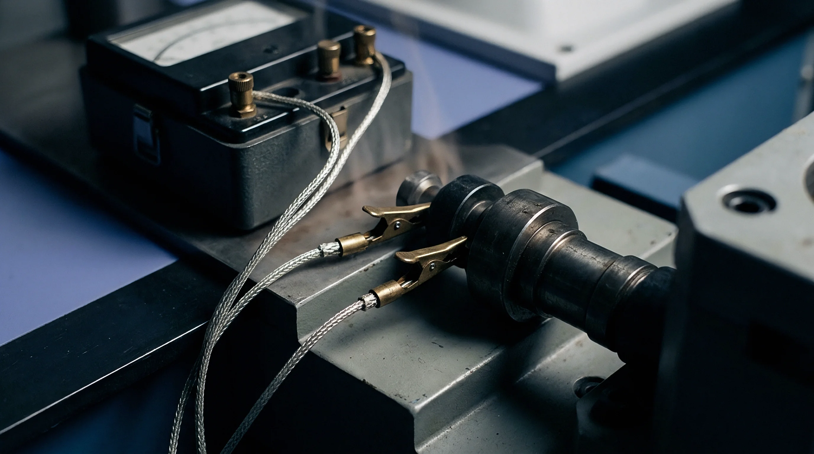
Evaluating operational amplifier stability under dynamic capacitive loads demands direct measurement of open-loop gain and phase response. Standard small-signal step response testing on an oscilloscope provides a fast visual check of overshoot, but fails to quantify exact phase margin or gain margin numbers under varied operating temperatures. Vector network analyzers equipped with wideband injection transformers allow non-invasive loop gain measurement inside a live feedback loop without breaking the DC operating point.

Vector Network Analysis of Phase Margin
Injecting a small-amplitude AC signal across a 50 Ω injection resistor inside the feedback loop reveals exact gain and phase margins under actual load conditions. The injection point must sit where the output impedance remains significantly lower than the input impedance of the feedback network. Plotting the Bode response across frequency surfaces hidden parasitic poles introduced by board layout, trace capacitance, and passive component non-idealities.
Compliance with IPC-7351B land pattern guidelines minimizes solder fillet asymmetry and associated mechanical stress on precision silicon dies.
Verification under temperature extremes exposes hidden stability failures caused by passive component drift. Multilayer ceramic capacitors with X7R or X5R dielectrics lose up to 60 percent of their nominal capacitance when operating near their rated DC voltage bias. This capacitance loss shifts the load-dependent pole to higher frequencies, unexpected altering the open-loop gain crossover point and degrading phase margin.
Cadence simulations miss parasitics. Reflow profile shifts zero location.
- Solder the target operational amplifier and associated passive components onto a low-loss test printed circuit board featuring 50 Ω controlled-impedance traces.
- Insert a 20 Ω non-inductive signal injection resistor into the primary feedback path between the output pin and the feedback junction.
- Connect wideband high-impedance active probes across the injection resistor to feed channels A and B of a vector network analyzer.
- Sweep the injection frequency from 10 Hz up to three times the expected unity-gain bandwidth while maintaining an injection amplitude below 10 mV peak-to-peak.
- Record the open-loop gain crossover frequency, phase margin at 0 dB gain, and gain margin at 180 degrees phase lag across the full operating voltage and temperature range.
How much phase margin degradation can a precision reference system tolerate before board-level manufacturing tolerances induce unexpected oscillations in high-volume production lines?

Trade
Silicon dies packaged in surface-mount housings exhibit varying thermal and mechanical stresses that affect long-term stability and reference drift. Quad Flat No-Lead and Dual Flat No-Lead packages provide small footprints and low lead inductance, but thermal expansion mismatches between the leadframe and the FR-4 substrate induce mechanical strain on the internal silicon die. Package thermal expansion shifts gain.
Solder stress shifts offset. This mechanical stress alters the piezoresistive characteristics of internal transistors, drifting the input offset voltage and changing open-loop output impedance over operational lifetimes.
Packaging Selection and Board Integration Costs
Selecting an MSOP-8 package over a DFN-8 footprint reduces assembly line re-work costs while increasing required PCB real estate by 45 percent. Gull-wing leaded packages like SOIC-8 and MSOP-8 absorb mechanical flex caused by thermal cycling or board bending, isolating the silicon die from external stresses. Small-outline no-lead packages solder directly to board copper pads via an exposed thermal pad, transmitting mechanical strain straight into the die substrate and shifting operational amplifier offset parameters.
| Package Type | Board Area (mm²) | Lead Inductance (nH) | Thermal Resistance (°C/W) | Delivered Price at 10k Units (USD) |
|---|---|---|---|---|
| 31.00 | 2.4 | 125 | 0.85 | |
| 15.00 | 1.5 | 180 | 1.12 | |
| 9.00 | 0.6 | 45 | 1.35 | |
| 2.56 | 0.2 | 90 | 1.78 |
Evaluating total landed cost requires factoring in assembly yield loss associated with microscopic packaging choices. Wafer-Level Chip-Scale Packages offer tiny footprints and minimal parasitic lead inductance, but demand tight stencil printing tolerances and automated optical inspection systems to avoid solder bridging. A failed solder joint on a bottom-terminated component requires manual hot-air rework, which subjects adjacent precision analog components to uncontrolled thermal spikes, altering their calibrated offset performance.
Specifying high-stability operational amplifier reference buffers involves balancing unit component cost against firmware compensation engineering overhead. Bare silicon dies mounted inside leaded plastic packages deliver moderate performance at low price points. High-precision applications demanding sub-ppm voltage stability require hermetically sealed ceramic packages or surface-mount modules with internal thermal shielding, driving the component unit cost up by a factor of ten while eliminating downstream software calibration routines on the production line.