Wafer Level Stress Distribution in Silicon Sensor Manufacturing
Thin-film stress gradients warp silicon sensor wafers, introducing overlay runout in steppers and severe bridge offset drift across piezoresistive diaphragms.

Bow
Mechanical distortion across single-crystal silicon substrates stems from the cumulative force of deposited thin films and backside thermal treatments. When net film force overcomes substrate rigidity, the circular wafer bends into spherical or cylindrical profiles, which fabs track by mapping surface deflection on three-point chuck fixtures or automated capacitive sensor grids. Tensile films ~ such as sputtered metals, thick silicon dioxide grown by wet pyrogenic oxidation, or heavily doped boron diffusion zones ~ pull the underlying crystal lattice inward into a concave bowl.
Conversely, compressive layers like silane-based PECVD films force excess atoms into interstitial spaces, expanding the surface and driving the wafer into a convex dome that lifts its edges off the reference plane.
Classical thin-film stress calculations rely on the Stoney relation to link substrate curvature directly to film tension. The formulation assumes spherical deformation, isotropic elastic behavior, and a uniform film that is orders of magnitude thinner than the substrate itself:
σf = (Es · hs2) / (6 · (1 – νs) · hf · R)
Here σf denotes the average thin-film stress, Es / (1 – νs) represents the biaxial elastic modulus of the silicon substrate, hs is substrate thickness, hf is total film thickness, and R represents the measured radius of curvature. In MEMS manufacturing, these assumptions quickly break down. Silicon sensors employ structural films whose thicknesses approach tens of micrometers, while substrate back-grinding reduces wafer thickness down to 100 or 150 micrometers.
When wafer deflection exceeds half the substrate thickness, deformation modes transition from linear bending into non-linear, anticlastic, or developable cylindrical topologies, causing the Stoney formula to underestimate local film stresses by 15 to 40 percent near wafer perimeters.
A 200-millimeter substrate carrying two micrometers of plasma silicon nitride at 400 degrees Celsius registers 380 megapascals of compressive stress.
Electrostatic and vacuum chucks pull warped substrates flat during processing, but clamping merely constrains the wafer without relieving stored strain energy. When high electrostatic voltages force a warped wafer against a rigid ceramic platen, that vertical warp converts directly into in-plane displacement. Once the chuck releases the substrate for cassette transit, the elastic deformation snaps back into its relaxed state, shifting surface patterns relative to prior lithographic levels.
| Layer Material | Deposition Method | Process Temperature (°C) | Intrinsic Stress Range (MPa) | Substrate Bow at 2 µm Film (µm) |
|---|---|---|---|---|
| Silicon Dioxide | Wet Thermal Oxidation | 1050 | -280 to -350 | 45 to 58 |
| Silicon Dioxide | PECVD TEOS | 390 | -120 to -180 | 19 to 29 |
| Silicon Nitride | LPCVD Dichlorosilane | 800 | +900 to +1200 | -145 to -195 |
| Silicon Nitride | PECVD Mixed Frequency | 350 | -150 to +200 | -24 to +32 |
| Polysilicon | LPCVD Silane Annealed | 620 | -50 to +50 | -8 to +8 |
| Aluminum Copper | Magnetron Sputtering | 200 | +180 to +260 | -29 to -42 |
Production lines monitor bow using full-surface optical deflectometry before committing wafers to deep reactive ion etching, where excessive warp disrupts backside helium cooling. If wafer bow exceeds 60 micrometers on an eight-inch substrate, peripheral helium seal leakage triggers localized thermal excursions that alter etch selectivity and stop active diaphragm releases.
Wafers showing visible edge curl in transfer cassettes typically lose lithographic overlay registration long before reaching the etch chambers.
Anisotropy
Crystalline silicon exhibits direction-dependent elastic constants that govern how mechanical deformation translates into electrical signals. Standard (100) wafers contain primary cubic axes along which stiffness changes with orientation: the Young modulus drops to a minimum of 130 gigapascals along <100>, climbs to 169 gigapascals along <110>, and peaks at 188 gigapascals along <111>. Because orientation dictates compliance, planar stress distributions warp wafers non-uniformly, turning isotropic film tension into anisotropic substrate strain profiles that distort circular dies into elliptical cross-sections.
Piezoresistive pressure sensors and inertial accelerometers exploit this directional sensitivity directly. Implanted p-type resistors positioned along the <110> direction of a (100) silicon diaphragm convert mechanical stress into fractional resistance shifts through piezoresistive coupling coefficients. When uniform radial stress profiles warp the host wafer, the electrical responses of identical test structures vary across the wafer map as shear components rotate the neutral axis.
Piezoresistive coefficients π11, π12, and π44 combine according to tensor transformation rules:
πl = 0.5 · (π11 + π12 + π44)
πt = 0.5 · (π11 + π12 – π44)
For p-type silicon, π44 dominates with a nominal value near +138 · 10-11 Pa-1 at room temperature, while π11 and π12 remain close to zero. Any parasitic shear stress introduced by wafer-level bending directly excites π44, generating uncommanded resistance changes in Wheatstone bridge legs before external measurands arrive at the sensor diaphragm.
| Wafer Surface Plane | Alignment Direction | Young Modulus (GPa) | Poisson Ratio | Dominant Piezoresistive Tensor | Transduction Efficiency |
|---|---|---|---|---|---|
| (100) | <110> | 169 | 0.062 | π44 (p-type) | High |
| (100) | <100> | 130 | 0.279 | π11, π12 (n-type) | Moderate |
| (110) | <110> | 169 | 0.250 | π11 + π12 + π44 | Very High |
| (111) | Arbitrary In-Plane | 188 | 0.262 | Isotropic In-Plane Group | Low |
Wafer warpage distorts sensor structures through several distinct physical failure channels:
- Diaphragm Premature Buckling occurs when compressive thin-film passivation overrides the tensile stiffness of micromachined membranes, driving mechanical bistability into pressure cells.
- Capacitive Gap Closure causes electrostatic combs in bulk-micromachined gyroscopes to drift toward static anchors, increasing parasitic pull-in sensitivity.
- Bridge Resistance Asymmetry forces orthogonal piezoresistive traces into unequal bias regimes, degrading common-mode rejection across nominal Wheatstone arrangements.
- Backside Cavity Tapering alters alkaline anisotropic wet etching rates along <111> sidewalls, yielding uneven diaphragm margins between center and edge dice.
Radial asymmetry across 200 mm wafers means that peripheral sensors experience substantial shear components compared to central dice that undergo predominantly equibiaxial stress. Wafer-scale calibration arrays must establish whether this spatial dispersion represents irreversible crystal plastic slip or recoverable elastic deformation that relaxes during die singulation.
Determining what proportion of perimeter die offset drift traces directly to wafer-scale crystallographic shear rather than local thin-film thickness non-uniformity remains critical for baseline process yields.

Thermal
Mismatch between the expansion coefficients of silicon substrates and surface passivations produces severe mechanical loads during furnace cooldown cycles. Silicon maintains a linear thermal expansion coefficient near 2.6 · 10-6 K-1 at room temperature. Chemical vapor deposition silicon dioxide features an expansion coefficient of 0.5 · 10-6 K-1, whereas sputtered aluminum metal lines sit near 23 · 10-6 K-1.
When wafers emerge from a 1000-degree thermal oxidation furnace or a 450-degree metallization alloy tube, differential contraction forces the composite structure into severe elastic distortion.
Do Multi-Layer Dielectric Stacks Cancel Net Curvature?
Alternating silicon dioxide and silicon nitride films targets a balance between tensile and compressive intrinsic components. Silicon dioxide grown under high-temperature thermal conditions remains intensely compressive at room temperature because the silicon substrate contracts substantially more than the oxide network during cooling. Silicon nitride grown through low-pressure chemical vapor deposition contracts less than its stoichiometric crystal density dictates, locking in tensile stresses approaching 1.2 gigapascals.
Process engineers pair these layers to build zero-curvature membrane composites.
Compressive dielectric layers buckle thin suspended diaphragms while tensile metallization pulls supporting anchors toward the chip center.
Balance calculations require meticulous parameter tuning. Assume a structural membrane stack on an 8-inch substrate containing 1.0 micrometer of thermal silicon dioxide with an intrinsic room-temperature stress of -320 megapascals, capped by low-pressure chemical vapor deposition silicon nitride with an intrinsic tensile stress of +950 megapascals. Setting total integrated film force to zero calculates the target nitride thickness:
Σ (σi · ti) = σox · tox + σnit · tnit = 0
(-320 MPa · 1.0 µm) + (+950 MPa · tnit) = 0
tnit = 320 / 950 ≈ 0.337 µm
Achieving total force cancellation prevents global wafer bow, yet local out-of-plane bending moments persist throughout the dielectric stack. The thermal silicon dioxide sits at the silicon interface, while the tensile silicon nitride rests on top. This spatial separation forms an internal bimorph structure.
When backside deep reactive ion etching removes the silicon handle wafer to suspend the sensor membrane, the internal moment releases, causing the edges to curl upward and shear thin membranes despite zero global wafer bow before cavity formation.
High-temperature wafer bonding adds severe thermal distortion challenges during hermetic sensor encapsulation. Anodic bonding seals silicon diaphragms against sodium-rich borosilicate glass substrates at temperatures between 350 and 450 degrees Celsius under 1000-volt electric fields. Although borosilicate glass matches the thermal expansion of silicon at 300 degrees Celsius, its expansion curve diverges sharply below 150 degrees.
Cooling bonded wafer pairs to 25 degrees Celsius freezes 80 to 120 megapascals of residual shear stress directly into the sealing glass frit or anodic interface, inducing long-term sensor scale-factor drift.
- Run incoming surface profilometry across unpatterned substrates to establish baseline raw wafer warp profiles.
- Deposit low-stress buffer oxides through high-density plasma deposition before initiating thick LPCVD structural runs.
- Subject intermediate dielectric layers to nitrogen furnace densification cycles at 900 degrees Celsius for 120 minutes.
- Measure post-anneal film curvature using multi-beam optical stress sensors to extract precise thermal expansion differentials.
- Strip backside sacrificial films through dry reactive ion etching to evaluate true single-sided composite forces.
- Adjust capping nitride gas ratios until substrate deflection returns to within 10 micrometers of the original baseline.
Failure to regulate these multi-layer thermal profiles warps wafers beyond downstream vacuum chuck tolerances, causing automated cassette transfer handlers to drop whole production lots onto chamber loadlocks.

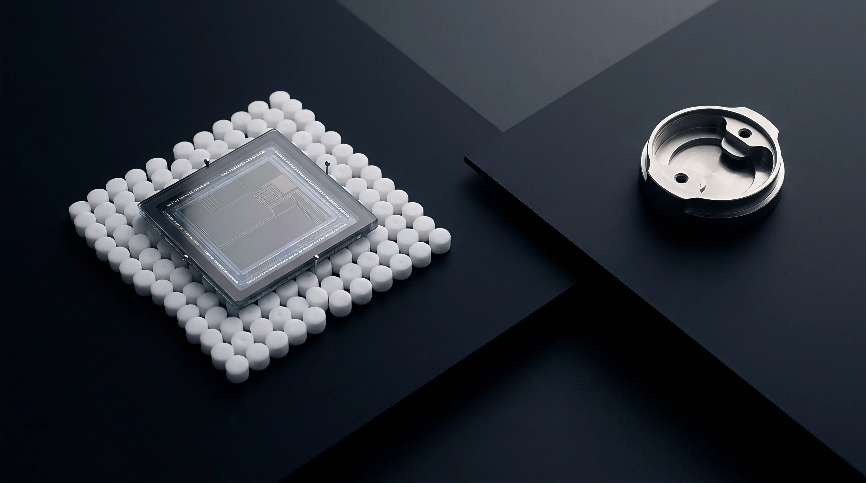
Lithography
Photolithographic exposure tools demand flat substrates within a tight focal plane depth to reproduce micron-scale sensor geometries. Advanced step-and-scan lithography systems deploy deep ultraviolet lasers with numerical apertures exceeding 0.75, yielding a usable depth of focus narrower than 400 nanometers. If residual film stress buckles a 200 mm wafer by 50 micrometers, vacuum chuck clamping cannot pull the warped edges entirely flat against the stage pin array.
The localized defocus produces severe critical dimension variations across etched piezoresistor lines, shifting their electrical sheet resistance by several percent between die rows.

Which Stepper Aligners Tolerate Local In-Plane Runout?
Exposure systems equipped with high-order grid correction compensate for field distortion induced by asymmetric substrate warpage. When a wafer undergoes unconstrained stress relaxation, points on the upper surface shift horizontally as well as vertically, creating in-plane distortion. Because steppers using standard six-parameter linear alignment models correct only for global wafer translation, rotation, and symmetric scaling, local in-plane runout eludes them completely, allowing pattern placement errors to accumulate radially across critical overlay margins.
SEMI M1 specifications enforce flat edge profiles to stop mechanical chuck runaway under variable film loads.
In-plane distortion scales with local curvature gradients across the wafer surface. A substrate exhibiting sudden localized stress variations, caused by patterned metal pads or deep oxide trenches, undergoes non-affine distortion during thermal chuck cycling. The absolute overlay error Δr follows the gradient of the out-of-plane deflection w(x,y):
Δr ≈ -0.5 · hs · ∇w(x,y)
For a 725-micrometer-thick wafer displaying localized deflection variations of 10 micrometers over a 20-millimeter exposure field, surface features displace laterally by up to 180 nanometers. This placement error consumes over half the allowable overlay budget for deep cavity contact hole alignments. Contact vias then land partially off their underlying diffused resistor pads, creating asymmetric contact resistances that destabilize bridge balance across temperature sweeps.
Backside lithography for through-wafer membrane formation faces even steeper overlay penalties. Alignment targets on the front surface must register against infrared or optical bottom-side microscopes through 400 micrometers of bulk silicon. Heavy bow creates prismatic optical distortion through the silicon substrate, displacing the visible optical target by several micrometers relative to true active features on the front surface.
Sensor diaphragms etch off-center relative to frontside piezoresistors, ruining device symmetry and inflating production rejection rates.
Unresolvable overlay drift frequently traces to customer layout patterns that violate global film symmetry across wafer quadrants, leaving stepper chucks unable to flatten the resulting saddle-shaped substrates.
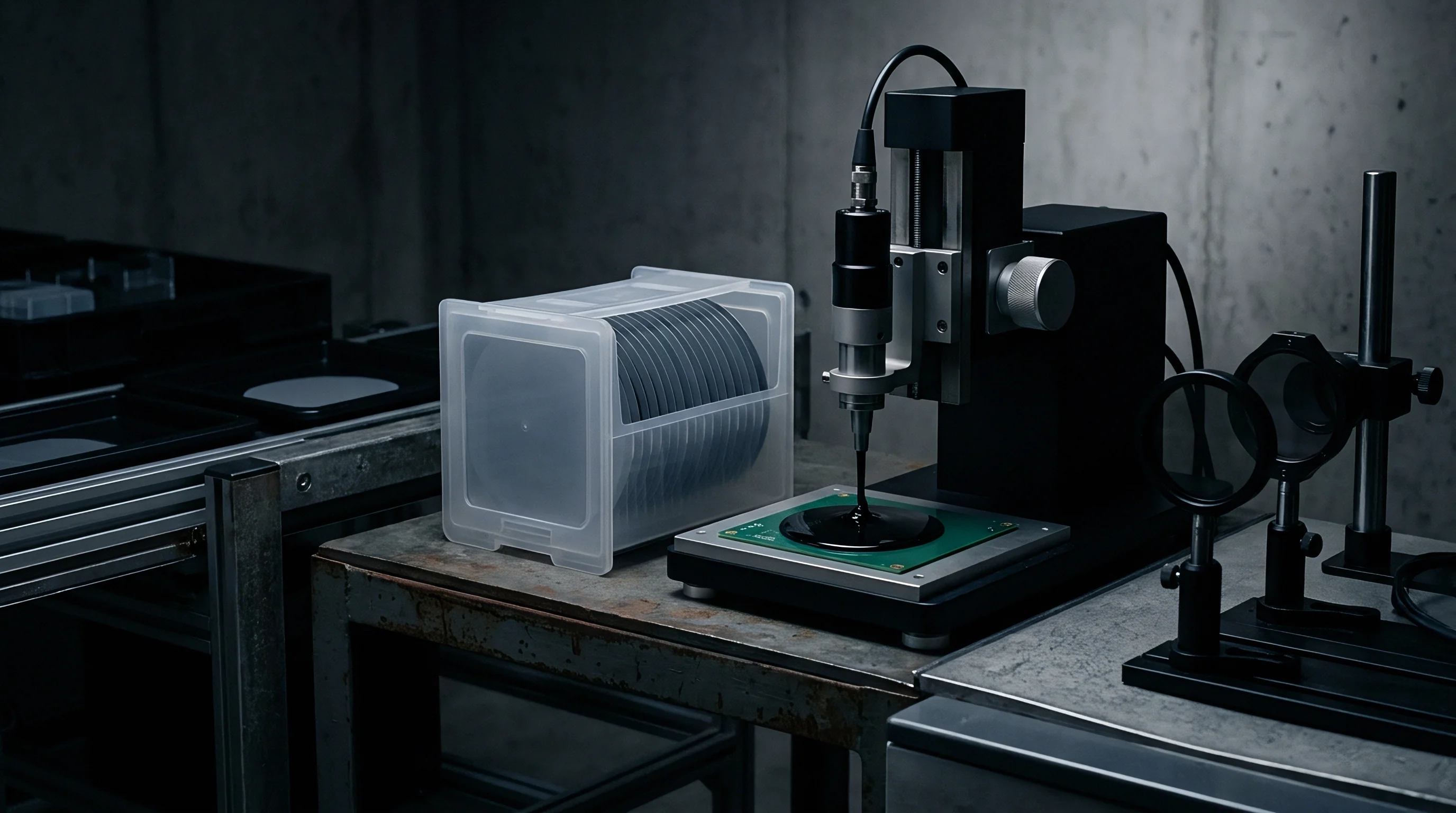
Offset
Zero-measurand signal bias represents one of the most sensitive indicators of residual mechanical force in micromachined sensors. In piezoresistive pressure transmitters, four resistors form a closed Wheatstone circuit on a thinned silicon membrane. Under zero external pressure, the differential bridge output voltage Vout divided by excitation voltage Vin should ideally equal zero millivolts per volt.
Residual film stresses, mounting forces, and non-uniform package encapsulation upset this electrical balance:
Vout / Vin = 0.25 · (ΔR1/R1 – ΔR2/R2 + ΔR3/R3 – ΔR4/R4)
Any non-uniform stress distribution across the membrane shifts individual resistance values independently. If local silicon nitride passivation stress varies by five megapascals across a 1-millimeter-wide diaphragm, the induced piezoresistive shift introduces an initial offset voltage exceeding 1.5 millivolts per volt, which consumes up to 15 percent of the full-scale signal budget in low-pressure industrial sensors.
Radial stress gradients translate directly into localized bridge voltage errors across adjacent die sites.
Temperature coefficients of offset present a more severe reliability hazard than room-temperature zero bias. While initial offset can be nullified by digital trimming inside host application-specific integrated circuits, stress-induced offset shifts non-linearly with operating temperature. Thermal expansion differentials between the silicon die, gold-tin or glass eutectic bonding interfaces, ceramic package substrates, and die-attach epoxies inject continuous mechanical loads directly into the sensing diaphragm, inducing hysteresis loops in zero-pressure readings over thermal excursions from -40 to +125 degrees Celsius.
Mitigating stress-induced bridge errors demands strict isolation architectures at the wafer level:
- Stress Relief Trenches etched completely through the silicon device layer decouple active sensing diaphragms from bulk peripheral substrate distortion.
- Symmetric Resistor Topologies layout designs place all four bridge elements in close spatial proximity along identical crystallographic axes, canceling common-mode stress gradients.
- Dummy Pattern Tiling surrounds sensitive active zones with inactive polysilicon and metal features, enforcing uniform chemical mechanical planarization rates and balanced surface tension.
- Compliant Eutectic Preforms absorb mounting strain through low-yield-strength solder alloys, mitigating package-induced stress transfer to the silicon die.
During mechanical drop tests or thermal shock sequences, unrelaxed wafer-level stresses facilitate microscopic dislocation glides within high-stress metal contact interfaces. This plastic slip alters baseline bridge resistance ratios permanently, manifesting as unrecoverable field calibration drift that fails sensor accuracy warranties long after shipment.
Standard master service agreements govern this vulnerability by enforcing SEMI M1 geometric flatness clauses alongside maximum allowable offset drift limits of 0.05 percent full-scale output following 1000 thermal cycles between -40 and +150 degrees Celsius.