Automated Thermal Burn in Acceleration Factors for Silicon Bridge Conditioning
Automated thermal burn in for silicon bridges balances Arrhenius-derived acceleration multipliers against microbump shear limits to weed out infant interconnect defects.

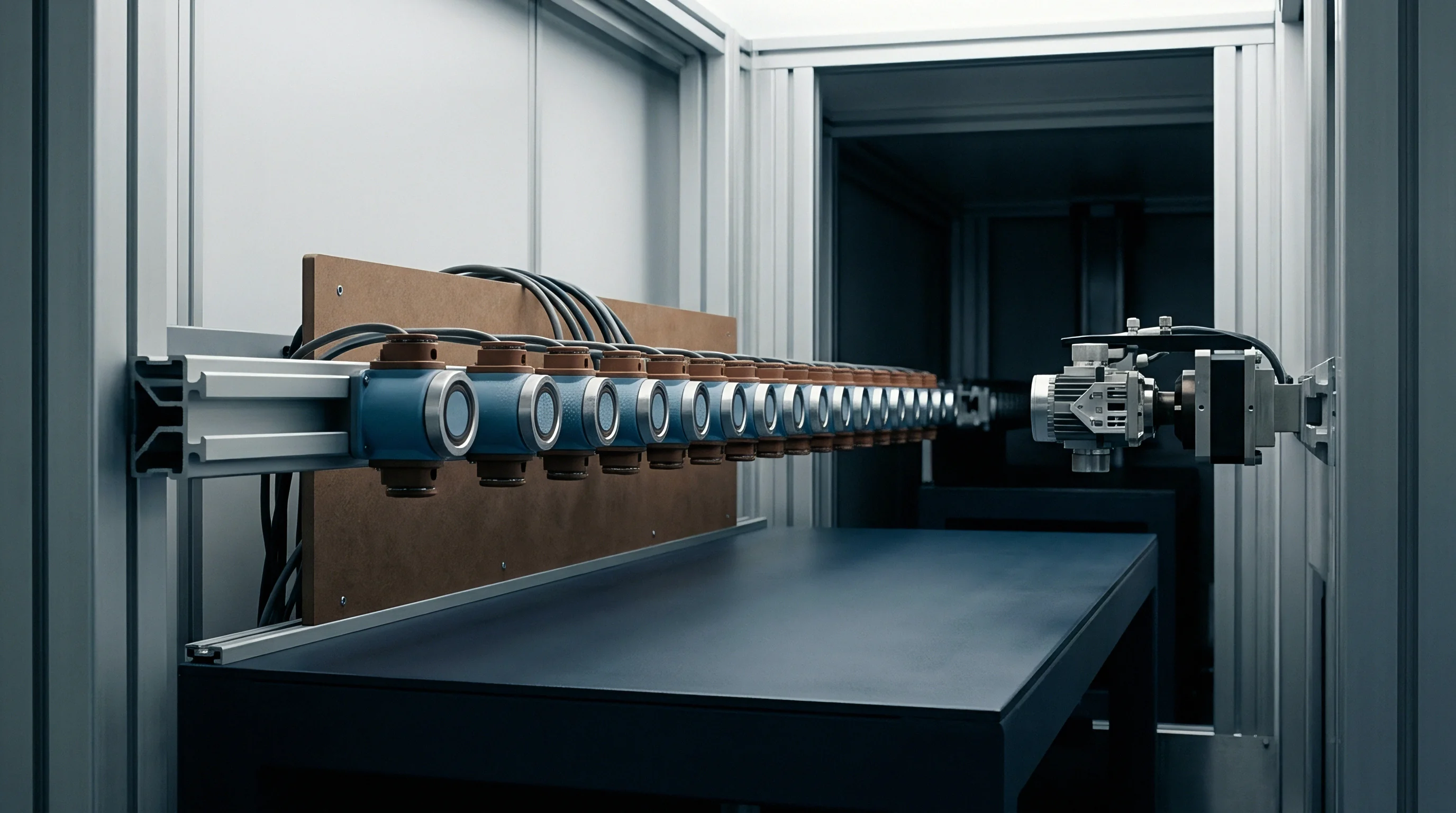
Gradient
Thermal dissipation across multi-die assemblies concentrates mechanical shear within localized interconnect boundaries. Embedded multi-die interconnect bridges rely on high-density microbumps with pitches below fifty-five micrometers to mate fine-pitch silicon routing to host package substrates, and failures routinely cluster along the perimeter bumps. The mismatch between bulk silicon’s thermal expansion coefficient at 2.6 parts per million per Kelvin and organic laminate build-up substrates at fourteen parts per million per Kelvin sets up chronic interfacial stress.
When package heaters ramp to conditioning setpoints, internal heat sinks and active bridges create localized junctions twenty to thirty-five degrees Celsius hotter than peripheral logic, altering atomic diffusion rates across these small-volume solder joints.
Automated thermal conditioning screens out latent infant mortality in the interconnect array before parts ship to field integration. Under active electrical continuity stress, thirty-micrometer copper-nickel-tin microbumps sustain current densities exceeding 104 amperes per square centimeter, concentrating current lines and triggering electro-migration alongside thermo-mechanical creep. Tin grain boundaries reorient rapidly as temperatures pass one hundred degrees Celsius, spurring intermetallic phases like Cu6Sn5 and Ni3Sn4.
Atomic flux divergences then coalesce into Kirkendall voids along trace boundaries, adding two milliohms to joint resistance.
Coalescence of Kirkendall voids within thirty-micrometer microbumps elevates interface resistance by forty percent after eighty hours at one hundred and thirty degrees Celsius.
Stress distributions during burn in depend heavily on the package architecture. In embedded bridge designs, cavity mold compounds maintain compressive force at room temperature but transition to tensile strain at sustained soak temperatures. This differential expansion strains the adhesive matrix, producing warpage that delivers mixed-mode peel stress straight into the outer bump rows.

Interconnect Failure Manifestations under Mechanical Shear
Elevated conditioning levels induce specific structural compromises across the bridge array:
- Intermetallic compound exhaustion consumes the thin-film under-bump metallization layer when thermal exposure outpaces typical storage boundaries, leaving brittle copper-tin boundaries susceptible to transverse fracture.
- Silicon cratering propagates beneath terminal interconnect pads as cyclical thermal expansion forces the rigid copper pillar into the underlying low-k dielectric stack.
- Underfill delamination initiates at bridge corner coordinates where peeling vectors exceed epoxy adhesion limits, severing localized structural reinforcement.
- Solder bridging develops across tight bump arrays when unconstrained eutectic volumes migrate through cracked passivations under sustained thermo-mechanical pressure.
Applying uncalculated conditioning profiles to multi-die bridges shears the outer perimeter microbumps, generating electrical open-circuit faults across wide bus interfaces during field assembly integration.

Formula
Mathematical acceleration models compress service lifetimes down to manageable chamber schedules by scaling operating hours against kinetic stress. Deriving usable test intervals requires treating each degradation mechanism with its own function. While classic Arrhenius relationships estimate thermal acceleration through apparent activation energy, Black’s equation incorporates current density to capture electrical bias.
For cyclic heating strains, modified Coffin-Manson or Norris-Landzberg formulations handle mechanical fatigue without introducing artifact failure modes.
What Thermal Stress Accelerates Silicon Bridge Aging?
Intermetallic growth kinetics follow an Arrhenius progression with empirical activation energies typically between 0.75 and 0.95 electron-volts, averaging roughly zero point eight electron-volts. The thermal acceleration factor scales with the Boltzmann constant, baseline operating temperature, and the elevated junction temperature sustained during burn in:
AFT = exp((Ea / k) × ((1 / Tuse) – (1 / Tstress)))
Assuming a baseline of sixty degrees Celsius and a stress dwell at one hundred and twenty-five degrees Celsius with an activation energy of 0.85 electron-volts, the calculated multiplier is approximately 168: one hour in the automated chamber corresponds to one hundred and sixty-eight hours in steady field service. When current travels through fine-pitch bridge traces, current crowding accelerates localized mass transport, which Black’s equation resolves through a current density term:
AFEM = (Jstress / Juse)n × exp((Ea,EM / k) × ((1 / Tuse) – (1 / Tstress)))
For flip-chip microbumps, the current exponent n falls between 1.5 and 2.0. Automated systems have to balance drive current against ambient chamber heating so joints do not reach liquidus or anneal sensitive silicon circuitry underneath.
The Arrhenius multiplier doubles every ten degrees until metallization transitions change the reaction mechanism entirely.
Cyclic thermal stress operates under different constraints, driving plastic deformation across the microbump solder joints as temperatures alternate. The Norris-Landzberg model accounts for both cycling frequency and temperature range:
AFNL = (fuse / fstress)m × (ΔTstress / ΔTuse)β × exp((Ea / k) × ((1 / Tmax,use) – (1 / Tmax,stress)))
The frequency exponent m hovers near 0.33, while the cycling exponent β runs close to 1.9 for low-lead and lead-free alloys. Pushing chamber temperatures too high in an effort to compress test cycles simply shifts the dominant failure mechanism from electro-migration to gross solder reflow.
| Mechanism | Governing Relationship | Activation Energy (eV) | Stress Exponent | Upper Temperature Limit (°C) |
|---|---|---|---|---|
| Intermetallic Growth | Arrhenius | 0.80 ± 0.05 | Not Applicable | 140 |
| Void Electromigration | Black Formulation | 0.90 ± 0.08 | 1.8 ± 0.2 | 130 |
| Thermomechanical Fatigue | Norris-Landzberg | 0.12 ± 0.02 | 1.9 ± 0.1 | 125 |
| Underfill Creep Voiding | Eyring Eyring Model | 0.65 ± 0.04 | 1.1 ± 0.1 | 115 |
Running chamber temperatures beyond 140 degrees Celsius shortens test dwell times, but it risks altering the active degradation physics and invalidating the mathematical acceleration altogether.
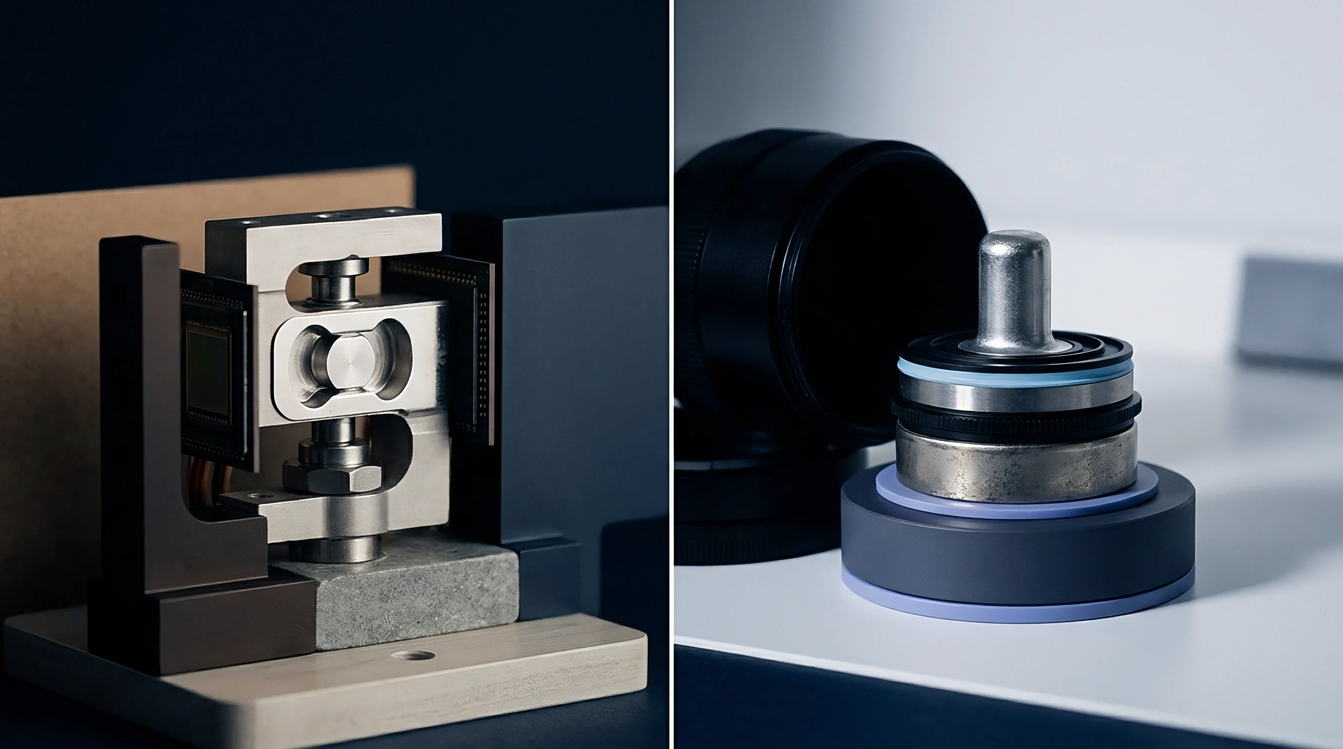
Socket
Automated test fixtures govern contact stability during rapid thermal transients. Automated conditioning relies on specialized sockets that clamp the package against temperature-controlled chucks to preserve uniform die temperatures. Inside the socket, contact pins experience aggressive mechanical scrub alongside recurring thermal expansion cycles.
Contact resistance drifts over time as contact springs lose yield strength under heat, copper pillar shear strength declines, and gold-plated pins begin oxidizing past eighty degrees.
Handling routines require strict sequencing to prevent spurious resistance failures while cycling under stress:
- Package insertion alignment brings package land grids into planarity with pogo contacts under regulated mechanical pre-loads.
- Thermal head docking compresses internal resistance heaters against the die backside lid with five hundred kilopascals of static pressure.
- Kelvin pin engagement verifies individual contact loops remain below twenty milliohms before activating bridge current loops.
- Chamber ambient elevation initiates thermal ramp rates controlled below three degrees Celsius per second to prevent thermal shock fracture.
- Current excitation applies regulated DC currents across designated power and return bumps on the silicon bridge.
- In-situ resistance monitoring polls four-point bridge structures every sixty seconds to record early phase drift.
- Controlled ramp-down lowers the unit to ambient room temperatures before pneumatic unclamp cycles trigger.
Automated test sockets degrade ten times faster under thermal cycling than under room-temperature sorting environments.
Replacing worn contactors costs upwards of twelve thousand dollars. As pins pick up solder residue transferred from substrate pads, localized tin-oxide films form and drive up contact resistance. That interface drop starves the bridge of its target stress current during burn in, letting under-conditioned silicon pass out of the cell as good product.
Worn contactors always show stable electrical resistance right up to the minute they burn a substrate land.


Margin
Measurement margins determine whether an interconnect has completed conditioning or suffered structural damage. Silicon bridges host dense parallel buses running at multi-gigabit speeds, where minute changes in bump resistance trigger impedance discontinuities, eye closure, and attenuation that push insertion loss outside specification. Resolving sub-milliohm shifts with four-point Kelvin sensing allows lines to separate benign lattice annealing from early void development.
Where Does Resistance Shift Threaten Bus Stability?
Bridge interconnects usually show an initial resistance drop between 0.5 percent and 1.5 percent over the first twelve hours of conditioning as grain structure settles and residual stresses relax in the bulk solder. After this initial anneal plateaus, continued thermal loading drives atomic migration and a steady rise in trace resistance. Any upward drift beyond five percent of that post-anneal baseline points to void nucleation.
| Uncertainty Contribution | Distribution | Standard Uncertainty (mΩ) | Sensitivity Coefficient | Combined Uncertainty (mΩ) |
|---|---|---|---|---|
| Instrumentation ADC Linear Error | Normal (k=2) | 0.045 | 1.0 | 0.0225 |
| Pogo Pin Thermal EMF Drift | Rectangular | 0.080 | 1.0 | 0.0462 |
| Temperature Coefficient of Trace | Normal (k=1) | 0.120 | 1.0 | 0.1200 |
| Socket Contact Scrub Repeatability | Rectangular | 0.065 | 1.0 | 0.0375 |
| Expanded Uncertainty (k=2, 95% Confidence) | Normal | Not Applicable | Not Applicable | 0.273 mΩ |
A rigorous acceptance evaluation requires disciplined screening criteria across every tested bridge channel:
- Trace baseline confirmation records initial dry-circuit resistance prior to applying thermal stress profiles.
- Thermal drift normalization subtracts the known resistance-temperature coefficient of internal copper routing from real-time measurements.
- Slope inflection monitoring flags circuits exhibiting positive second derivatives in resistance trends over four consecutive readout intervals.
- Isolation integrity checks test inter-trace dielectric resistance at five hundred volts per mil to catch dendrite formation.
Whether sub-milliohm shifts observed across intermediate test dwells represent reversible lattice adjustments or irreversible structural fatigue remains difficult to arbitrate without destructive physical cross-sectioning.

Yield
Packaging margins balance chamber dwell against fallout exposure. Running long conditioning profiles ties up expensive sockets and caps plant throughput, while shortening cycles risks field dead-on-arrival rates that inflate warranty reserves. On multi-chip modules carrying three to six silicon bridges, an escape rate of fifty parts per million per bridge multiplies into module scrap that quickly erodes profitability.
Perimeter microbumps remain the primary failure point when bridge assemblies endure excessive mechanical soak. In automotive and enterprise compute procurement, supply agreements enforce rigid qualification gates, forcing test engineers to balance socket wear against defect screening coverage. Standard forty-eight-hour dwells at one hundred and twenty-five degrees Celsius routinely absorb five to eight percent of package gross margin in fixture maintenance and depreciation alone.
Contract stipulations governing multi-die burn in mandate that suppliers absorb total module replacement costs whenever bridge fallout exceeds fifty parts per million during customer board integration.
High-density packaging floors increasingly use active thermal control systems equipped with independent heater pedestals at each die position. When dies on a shared substrate vary in size, handling hardware must adjust mechanical clamping force and thermal output on the fly. An uncalibrated pedestal creates hot spots that over-age one bridge while leaving an adjacent link under-screened, scattering reliability numbers across units from the very same wafer lot.
JEDEC standard JESD22-A108 specifies high-temperature operating life parameters, dictating that stress junction temperatures maintain accuracy within plus or minus five degrees Celsius across all active channels to retain test validity.