Wafer Level Strain Isolation Decoupling Architecture Limits under Cryogenic High Vibration Environments
Wafer level strain isolation requires tuning micro-machined silicon flexure tethers to absorb thermal contraction while keeping natural frequencies above excitation bands.
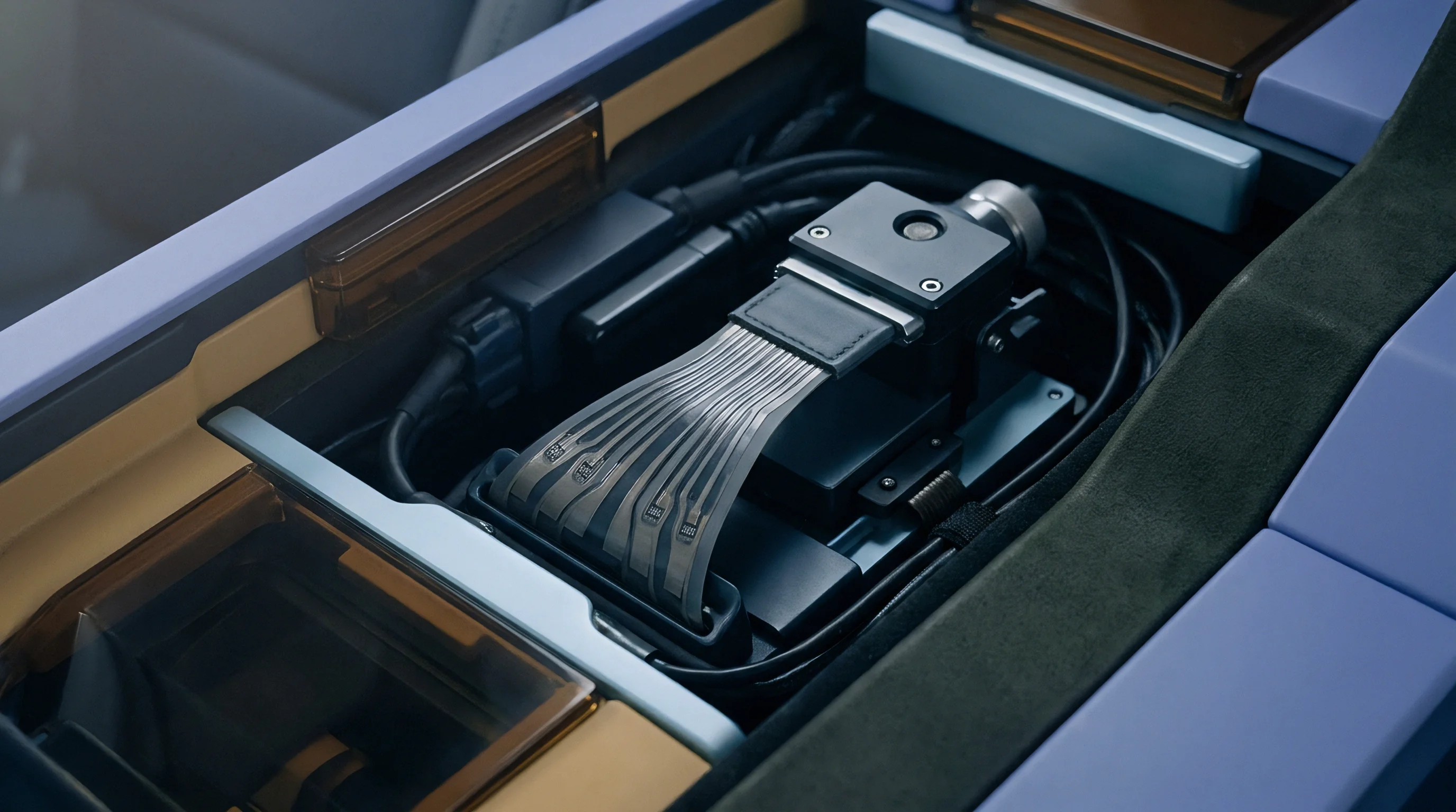

Frost
Cooling a silicon sensor die from ambient room temperature down to 4.2 Kelvin induces severe mechanical stress across the packaging interface due to differential thermal contraction. Silicon exhibits an integrated thermal contraction of approximately 0.04 percent when cooled from 293 Kelvin to 4 Kelvin. Common packaging substrate materials contract at substantially higher rates over the same thermal span.
Borosilicate glass contracts by 0.10 percent, alumina ceramics by 0.11 percent, and copper backing plates by 0.32 percent. Organic die-attach adhesives and polymers exhibit total thermal contraction figures exceeding 1.2 percent. When these heterogeneous materials join at elevated cure temperatures, cryogenic operation freezes this expansion mismatch into permanent physical strain.
Material properties shift continuously along the thermal drop. Yield strengths increase, ductility drops to zero, and mechanical compliance vanishes in organic buffers. Cold shifts material stiffness.
Polymer adhesives undergo glass transition during cooling, rising in storage modulus from 2 gigapascals at room temperature to over 8 gigapascals at 77 Kelvin. The brittle material behavior prevents stress relaxation through plastic flow. Consequently, interfacial shear stresses concentrate at die corners and bond boundaries, transmitting bending moments directly into active sensor diaphragms.
Thicker compliant interlayers lower thermal strain transmission across heterogeneous materials while shifting the mechanical resonance into lower frequency bands.
Wafer-level strain isolation architectures insert mechanical decoupling interfaces between the carrier substrate and the sensing die during fabrication. Without these isolation structures, differential contraction deforms the silicon crystal lattice. Lattice deformation alters the physical dimensions of capacitive gaps and changes the carrier mobility of piezoresistive elements.
In high vibration environments, static cryogenic thermal strain combines with dynamic excitation stress, pushing interfacial shear beyond bond adhesion limits.
The table below details material property shifts across operating temperature regimes from ambient down to liquid helium temperatures.
| Material | Temperature (K) | Young’s Modulus (GPa) | Mean CTE (10^-6 / K) | Integrated Contraction (%) |
|---|---|---|---|---|
| Single Crystal Silicon (100) | 293 | 130 | 2.6 | 0.00 |
| Single Crystal Silicon (100) | 77 | 133 | 0.8 | 0.03 |
| Single Crystal Silicon (100) | 4 | 135 | 0.01 | 0.04 |
| Borosilicate Glass 7740 | 293 | 64 | 3.25 | 0.00 |
| Borosilicate Glass 7740 | 77 | 68 | 1.1 | 0.08 |
| Borosilicate Glass 7740 | 4 | 70 | 0.05 | 0.10 |
| Eutectic Au-Sn (80/20) | 293 | 59 | 16.0 | 0.00 |
| Eutectic Au-Sn (80/20) | 77 | 68 | 10.2 | 0.28 |
| Eutectic Au-Sn (80/20) | 4 | 71 | 1.5 | 0.34 |

Thermoelastic Shear Stresses in Glass and Silicon Substrates
Interfacial shear stress scales linearly with substrate width and thermal expansion divergence. Analytical modeling of a two-layer bonded strip reveals that peak shear stress occurs within one edge-distance zone from the die boundary. For a 5 millimeter silicon die bonded directly to a glass carrier with a 25 micrometer gold-tin eutectic solder layer, cryogenic cooling generates localized shear stresses exceeding 120 megapascals at the perimeter.
This localized stress field propagates strain energy through the substrate depth into active surface microstructures.
Direct die attachment causes severe sensor performance degradation at low temperatures. Unisolated sensing elements suffer from baseline offset shifts, gain drift, and enhanced microphonic sensitivity. High dynamic acceleration inputs aggravate these effects by modulating interfacial shear stresses.
Microscopic cracks nucleate at solder voids and glass interfaces under combined static and dynamic load profiles. Isolating the sensing structure at the wafer level requires introducing geometric compliance that absorbs thermal expansion mismatch while maintaining structural rigidity along critical measurement axes.
The failure modes listed below occur when rigid wafer bonding architectures undergo cryogenic temperature drops.
- Interfacial Delamination Unbonding spreads along the metal solder or adhesive interface when perimeter shear stress exceeds local bond adhesion strength.
- Die Warpage and Cracking Out-of-plane bending moments induce high tensile stresses across the back surface of the silicon die, triggering brittle catastrophic fractures.
- Piezoresistive Zero Offset Shift Unbalanced thermal strain shifts Wheatstone bridge resistance values, exhausting downstream electrical compensation range.
- Capacitive Gap Distortion Differential thermal contraction alters parallel plate spacing, creating non-linear capacitance responses to baseline excitation.
Thinner bond lines reduce thermal gradient delays across heterogeneous die stacks while increasing direct stress transfer into sensitive sensor areas.


Flexure
Engineered structural suspensions isolate active wafer regions by interposing localized mechanical compliance between the carrier frame and sensor island. Micro-machined flexures carved directly into the silicon substrate serve as high-pass spatial filters for strain. These flexure arrays permit differential thermal expansion between the outer mounting ring and the central sensor island through bending and torsional deformation of narrow silicon beams.
The dimensions of these compliance elements determine both the strain isolation factor and the dynamic load capacity.
Silicon flexures operating at cryogenic temperatures exhibit elevated mechanical spring constants. The Young’s modulus of single-crystal silicon increases by approximately 3.8 percent when cooled from room temperature to 4.2 Kelvin. Silicon becomes brittle.
This modulus increase stiffens compliant suspension beams, elevating the primary mechanical resonant frequency of the decoupled island assembly. Designers must size beam widths and lengths to accommodate this cryogenic stiffening effect without exceeding material tensile limits under dynamic acceleration inputs.
Mechanical Transfer Functions of Compliant Silicon Tethers
Mechanical strain transmission across a tethered island architecture follows a second-order spring-mass-damper transfer function. The strain attenuation ratio depends on the relative stiffness between the suspension flexures and the internal sensor island. Folding the flexure geometry into serpentine or S-shaped beam configurations increases mechanical compliance within a compact footprint.
A folded tether with length L, width w, and thickness t provides an in-plane spring constant proportional to the cube of the width-to-length ratio.
Deep reactive ion etching forms vertical sidewalls that define flexure cross sections with high aspect ratios. Etch depth uniformity controls suspension symmetry across six-inch and eight-inch wafer surfaces. Thickness variations of 5 percent across a wafer produce a 15 percent spread in flexure spring constants.
This spread shifts the strain isolation performance across die locations, altering individual sensor rejection ratios.
| Architecture Type | Strain Isolation (dB) | Resonant Frequency (kHz) | Thermal Resistance (K/W) | Shock Limit (g) |
|---|---|---|---|---|
| Etched Through-Silicon Tether Array | 38 to 46 | 2.4 to 5.1 | 450 to 1200 | 1200 |
| Polyimide Compliant Bump Array | 18 to 26 | 8.5 to 14.2 | 80 to 220 | 3500 |
| Substrate Cavity Back-Etch Membrane | 28 to 34 | 1.1 to 3.2 | 310 to 680 | 800 |
| Suspended Silicon-on-Insulator Island | 42 to 52 | 3.8 to 8.6 | 850 to 2100 | 1500 |
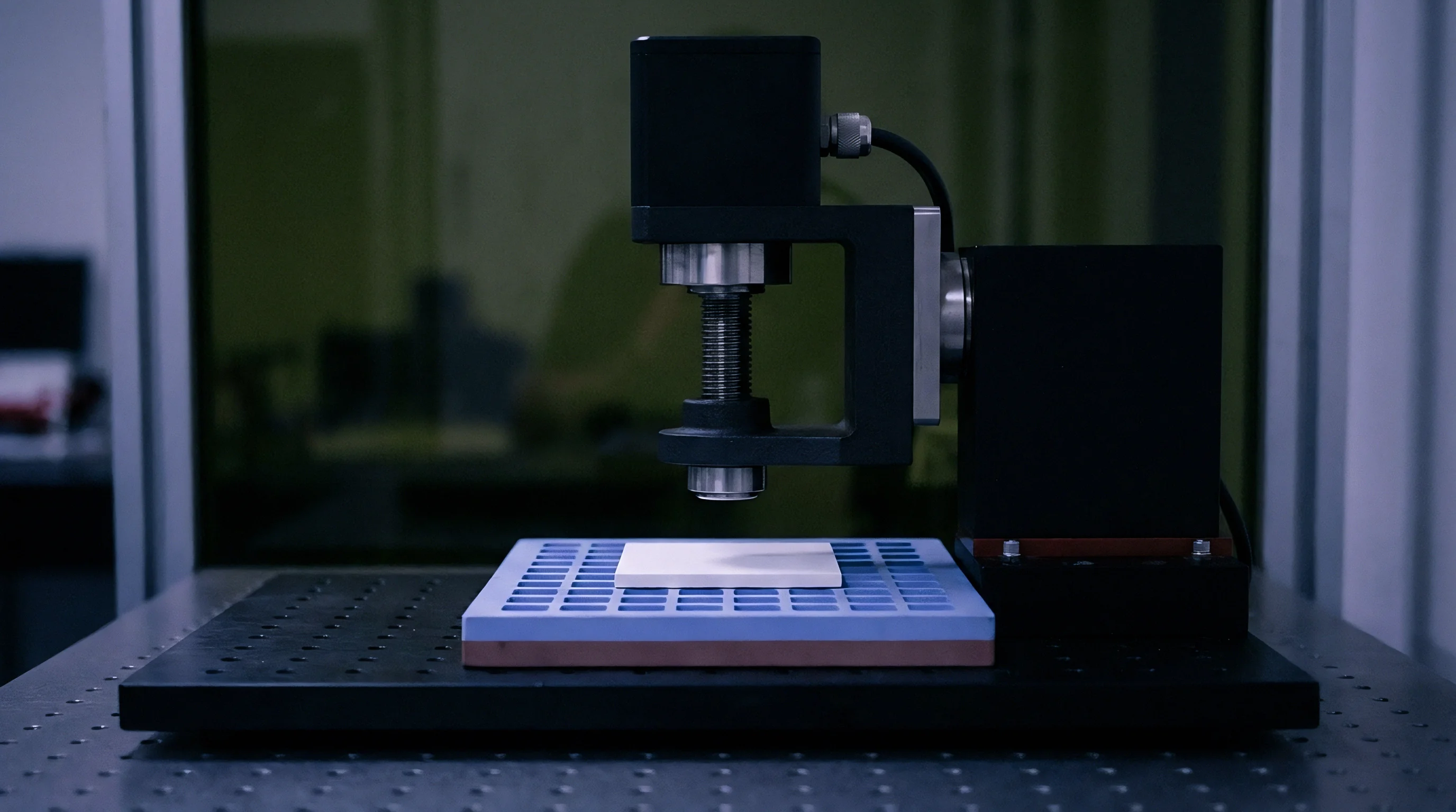
Micro Structural Decoupling Geometries
Silicon-on-insulator wafers provide precise vertical dimension control for strain-decoupling structures. The buried oxide layer acts as an etch stop during deep reactive ion etching, fixing the flexure thickness to the top device layer dimension. Island structures formed in 30 micrometer thick device layers maintain high out-of-plane stiffness while yielding high in-plane compliance.
This dimensional selectivity suppresses out-of-plane translational displacement during vertical vibration exposure.
At 77 Kelvin, a folded single-crystal silicon tether array achieves 42 decibels of mechanical strain attenuation for in-plane carrier deformation.
Polymer bump decoupling architectures offer an alternative to etched silicon tethers. Photosensitive polyimide or benzocyclobutene pillars deposited between the substrate and sensor die absorb thermal expansion mismatch. At cryogenic temperatures, polymer stiffness rises dramatically, reducing strain isolation efficacy.
Silicon flexure architectures avoid polymer glass transition issues, maintaining predictable linear elastic behavior down to millikelvin temperatures.
Wafer foundries frequently state that micro-machined flexure arrays introduce unmanageable handling yields during back-end grinding and dicing steps.


Dynamics
Random mechanical excitation transmitted through cryogenic cooling stages excites structural resonances within the wafer isolation suspension. Cryogenic environments like liquid helium dewars and closed-cycle pulse tube cryocoolers present intense dynamic vibration spectrums. Cryocoolers produce fundamental pressure pulses between 1 Hz and 3 Hz alongside high-frequency harmonic vibrations extending up to 2000 Hz. Broadband random vibration levels frequently reach 20 g RMS in aerospace and launch vehicle instrumentation platforms.
Internal material damping collapses at low temperatures. Material loss factors for single-crystal silicon drop from 10^-4 at room temperature down to below 10^-7 at temperatures under 20 Kelvin. Damping collapses at four Kelvin.
Without ambient gas dissipation inside vacuum-encapsulated wafer cavities, mechanical quality factors (Q) of suspended silicon islands jump from 500 at atmospheric room temperature to over 100,000 in cryogenic vacuum chambers. This Q-factor escalation severely amplifies structural motion at the suspension natural frequency.

What Dynamic Amplification Limits Compliant Silicon Springs at Cryogenic Temperatures?
Dynamic amplification at resonance equals the mechanical quality factor Q. A 20 g RMS broad-band vibration input containing spectral density at the flexure natural frequency generates extreme dynamic displacements when Q reaches 50,000. Under these conditions, a flexure designed to isolate low-frequency thermal strains experiences dynamic stress amplification that exceeds the fracture strength of silicon. Compliant tethers isolate thermal strains.
High dynamic loads induce fatigue fractures.
The total dynamic displacement scales inversely with the square of the resonant frequency. Lowering flexure stiffness improves thermal strain isolation but shifts the system natural frequency down into the peak power spectral density region of environmental vibration. This trade-off establishes an operational boundary for cryogenic strain isolation architectures.
Isolation structures must maintain their fundamental resonant frequency above maximum environmental excitation frequencies while providing sufficient compliance to attenuate thermal stresses.
Verification under IEC 60068 2 64 demands continuous random vibration exposure across the 20 Hz to 2000 Hz band without mechanical resonance structural yield or phase shift.

Viscous and Thermoelastic Damping Collapse
Thermoelastic dissipation serves as the primary intrinsic damping mechanism in micro-scale silicon flexures at room temperature. Thermoelastic damping occurs when flexural bending creates thermal gradients across the beam thickness, causing irreversible heat flow. As temperature approaches absolute zero, the coefficient of thermal expansion approaches zero, and specific heat capacity drops following a T-cubed relationship.
These physical shifts reduce thermoelastic dissipation to zero, removing intrinsic material damping.
Extrinsic damping mechanisms must compensate for thermoelastic damping loss to prevent destructive resonant amplification. Active squeezed-film gas damping cannot operate at cryogenic temperatures due to helium condensation and vacuum sealing requirements. Alternative damping mechanics rely on thin-film metal coatings applied to flexure surfaces.
Depositing a 100-nanometer gold or platinum film over silicon beams introduces interfacial viscoelastic friction that caps maximum Q factors below 2,000 at 4 Kelvin, limiting dynamic amplification.
The sequence below details mechanical energy transfer and amplification during random vibration exposure.
- Base Excitation Energy Input Broad-band mechanical vibration enters the sensor package through carrier mounting points.
- Flexure Frequency Selective Filtering Suspension tethers attenuate frequencies above the fundamental resonance while passing low-frequency motion.
- Resonant Energy Accumulation Input energy matching the structural resonant frequency accumulates due to ultra-low cryogenic material damping.
- Dynamic Stress Concentration Accumulated motion focuses high cyclic bending stresses at tether anchor roots.
- Transduction Signal Modulation Dynamic displacement alters internal sensor gaps, introducing dynamic noise artifacts into signal output channels.
The operational ceiling where dynamic damping controls resonant displacement without adding low-temperature thermal conduction channels remains unresolved for sub-10 Kelvin sensor platforms.


Shift
Parasitic deformation reaching the active sensing element alters internal crystal lattices and changes zero-load signal baseline measurements. Piezoresistive sensor elements rely on piezoresistive coefficients to convert strain into electrical signals. Unisolated mechanical strain induced by packaging contraction modulates these coefficients directly.
Piezoresistive coefficients increase significantly as temperature drops. The piezoresistive coefficient pi-44 in p-type silicon increases by more than 200 percent at 77 Kelvin compared to room temperature values, magnifying parasitic strain sensitivity.
Piezoresistive bridge circuits suffer from severe thermal zero-drift when unisolated strain fields are asymmetrical. Dynamic strain distorts Wheatstone bridges. Random vibration inputs generate dynamic mechanical strains that mix with static thermal contraction fields.
This strain combination causes signal saturation in high-gain preamplifiers, degrading measurement resolution and dynamic range.
Piezoresistive Coefficient Modulation under Dynamic Strain
Parasitic strain field changes alter the band structure of silicon, shifting hole and electron mobility across crystal axes. In a four-arm Wheatstone bridge, isotropic strain shifts all resistor arms equally, yielding minor offset changes. Asymmetrical strain fields produced by corner stress concentrations in unisolated dies alter individual bridge arms differently.
This imbalance causes zero-load output shifts exceeding 30 millivolts per volt of excitation at cryogenic temperatures.
Dynamic vibration modulates this zero shift at the vibration frequency. When random vibration acceleration acts on the sensor die, package-induced strain fields shift dynamically due to micro-slippage at mounting interfaces. This micro-slippage creates non-repeatable hysteresis loops in sensor offset curves during thermal cycling.
| Error Source | Unisolated Sensor (% FSO) | Tether Isolated Sensor (% FSO) | Isolation Efficacy |
|---|---|---|---|
| Static Thermal Contraction Shift | 18.40 | 0.85 | 21.6 x reduction |
| Dynamic Vibration Cross-Sensitivity | 6.20 | 0.42 | 14.8 x reduction |
| Hysteresis Across Thermal Cycles | 3.10 | 0.12 | 25.8 x reduction |
| Resonant Peak Output Distortion | 12.50 | 1.15 | 10.8 x reduction |
| Total Combined Signal Offset Error | 40.20 | 2.54 | 15.8 x reduction |
Capacitive Comb Finger Deflection and Signal Distortion
Capacitive MEMS sensors detect physical displacement by measuring capacitance changes between interdigital comb fingers. Parasitic packaging strain deforms the frame holding stationary comb fingers, shifting baseline capacitance without external acceleration. In a cryogenic environment, a frame strain of 100 microstrain alters inter-element gap distances by several nanometers, driving baseline capacitance shifts that mimic actual signal inputs.
Residual stress from cryogenic package contraction shifts the baseline output of piezoresistive Wheatstone bridges by more than twenty percent of full scale output.
High-g dynamic vibration causes lateral deflection of compliant comb structures. When external vibration frequencies align with cross-axis isolation modes, comb fingers move off-axis, introducing non-linear electrostatic attraction forces. These non-linear forces cause snap-in instabilities, short-circuiting capacitive sensing elements.
Robust wafer isolation architectures must keep cross-axis mechanical deflection below 5 percent of nominal gap width under maximum dynamic vibration levels.
Evaluating strain sensitivity on cryogenic shake tables requires a sequential qualification process.
- Mount the unpowered wafer module into a liquid helium cryostat attached to an electrodynamic shaker table.
- Cool the test setup down to 4.2 Kelvin at a maximum rate of 2 Kelvin per minute to prevent thermal shock fractures.
- Measure static electrical offset shifts across Wheatstone bridge terminals at stable base temperatures.
- Apply broad-band random vibration from 20 Hz to 2000 Hz at 5 g RMS increments up to 20 g RMS.
- Record real-time noise density spectra and zero-shift offset deviations during active vibration exposure.
- Cycle the cryogenic chamber back to room temperature and re-verify zero-load electrical baselines to check for micro-slip hysteresis.
Selecting an unisolated packaging architecture forces downstream signal acquisition electronics to absorb non-linear offset shifts that exceed the input range of low-noise preamplifiers.


Fracture
Single-crystal silicon exhibits complete absence of plastic deformation below 100 Kelvin, causing stress concentrations at geometric transitions to initiate rapid structural failure. The brittle-to-ductile transition temperature for silicon sits near 800 Kelvin. Below this threshold, dislocations remain frozen inside the crystal lattice.
At cryogenic temperatures, crack propagation occurs purely through cleavage along low-index crystallographic planes, primarily the (111) and (110) orientation directions.
Critical stress intensity factors (K1c) define material resistance to brittle fracture. Single-crystal silicon exhibits a K1c fracture toughness between 0.9 and 1.2 MPa square-root meters at room temperature. At liquid helium temperatures, fracture toughness drops by 10 to 15 percent along specific cleavage planes.
Parasitic strain stress peaks combining with dynamic vibration bending stresses easily exceed the critical threshold at micro-structural defect sites.
Stress Concentration at Deep Reactive Ion Etching Notch Roots
Deep reactive ion etching processes leave surface roughness and scalloping profiles along etched sidewalls. The depth and radius of these etch scallops determine local mechanical stress concentration factors. A scallop radius of 50 nanometers at a flexure root increases nominal bending stresses by factors of 3 to 5.
Etch scalloping forms notch roots. Fracture toughness drops at four Kelvin.
Micro-cracks nucleate at these high-stress notch roots during dynamic vibration loading. Under cyclic vibration exposure at cryogenic temperatures, silicon does not experience classic dislocation-based fatigue. Silicon micro-structures suffer from environmentally assisted slow crack growth and sub-critical micro-fracture propagation along surface defect lines.
Cumulative stress cycles gradually extend micro-cracks until the remaining cross section fails catastrophically under peak dynamic loads.
Corner Radius Optimization for Cryogenic Silicon Suspension Beams
Sharp internal corners inside micro-machined flexure anchors generate theoretical stress singularities. Sizing anchor fillet radii properly distributes bending stress smoothly into surrounding frame structures. Analytical stress calculations confirm that internal fillets with radii exceeding twice the beam width reduce peak anchor stress levels below 200 megapascals under 20 g RMS dynamic load conditions.
Surface passivation treatments clear micro-etch pits and smooth scalloping features along etched beam walls. Anisotropic wet etching with potassium hydroxide or tetramethylammonium hydroxide yields atomical flat (111) sidewall planes free from mechanical notches. Photolithographic mask alignment errors create micro-steps along wet-etched features, forming stress concentrators.
Wafer isolation designs must incorporate generous safety margins on allowable yield stresses.
The checklist below specifies structural design criteria for cryogenic silicon flexure reliability.
- Anchor Fillet Radii Fillet radii at beam connections must exceed two times the nominal beam width to eliminate corner stress singularities.
- Sidewall Roughness Limits Deep reactive ion etch sidewall scalloping depth must remain below 30 nanometers across the entire flexure profile.
- Wafer Orientation Alignment Primary flexure bending axes must align with crystallographic directions possessing higher fracture toughness values.
- Etch Stop Profile Control Transition zones near buried oxide layers must remain free from micro-trenching defects during plasma etching steps.
Standard qualification testing under MIL-STD-883K Method 2002.5 condition B rejects component lots that exhibit micro-fracture propagation across flexure anchors following shock exposure.


Margin
Commercial adoption of wafer-level isolation architectures depends on maintaining acceptable die yields across complex etched flexure processes. Manufacturing compliant strain isolation structures requires adding process steps to standard MEMS fabrication flows. These steps include double-sided deep reactive ion etching, cavities etched into handle wafers, alignment of silicon-on-insulator layers, and hermetic wafer-to-wafer bonding.
Yield loss scales with flexure depth.
Wafer handling presents severe shock hazards. Thin, compliant flexures etched directly into production wafers render substrates fragile during spin-coating, automated pick-and-place, and dicing operations. Substrate fragility forces foundries to utilize temporary carrier wafers held together by cryogenic-compatible waxes or mechanical frame clamps, adding process complexity and manufacturing cost.
Wafer Level Packaging Cost and Yield Tradeoffs
Fabrication costs scale non-linearly with mask count and etch depth precision. Incorporating wafer-level strain isolation adds between 35 and 60 percent to total raw wafer processing costs compared to standard non-isolated sensor dies. Yield drops occurring during deep silicon etching and dicing operations drive final landed costs even higher.
Individual die yields for suspended island architectures typically average between 68 and 82 percent across a six-inch production wafer.
Savings achieved during downstream system integration offset elevated wafer fabrication costs. Integrated wafer-level strain isolation eliminates the need for complex, custom-machined discrete mechanical isolation dampers inside the cryogenic sensor housing. System integration labor, calibration time, and hand-assembly yield losses decline when strain isolation is built directly into the silicon die structure.

Qualification Metrics for Cryogenic Sensor Foundations
Qualifying a cryogenic sensor isolation architecture requires verifying performance across combined thermal, mechanical, and electrical stress regimes. Component lots must complete multiple thermal shocks between ambient and 77 Kelvin without structural failure or bond line degradation. Qualification protocols specify continuous exposure to random vibration across three orthogonal axes while operating at cryogenic base temperatures.
Sourcing pools for specialized cryogenic MEMS manufacturing remain restricted. Only a limited group of specialized MEMS foundries possess double-sided deep silicon etching capabilities alongside wafer-level cavity hermetic sealing processes. Buyers must evaluate foundry capabilities using standardized test vehicles to verify etching uniformity, sidewall roughness limits, and bond interface integrity before committing to volume production runs.
Foundries capable of delivering deep silicon flexure etching combined with cryogenic metallization operate under tightly allocated schedules, requiring buyers to lock in wafer design parameters eighteen months ahead of full volume production.