Geometric Deviation
Out-of-plane distortion occurs when internal stresses in a composite laminate exceed its structural stiffness. Such board warping typically appears as a bow or twist across the surface of a printed circuit board. This condition results from an imbalance in the distribution of copper layers.
It remains within acceptable limits if the vertical displacement does not interfere with the planarity required for automatic component placement.
Metrological Assessment
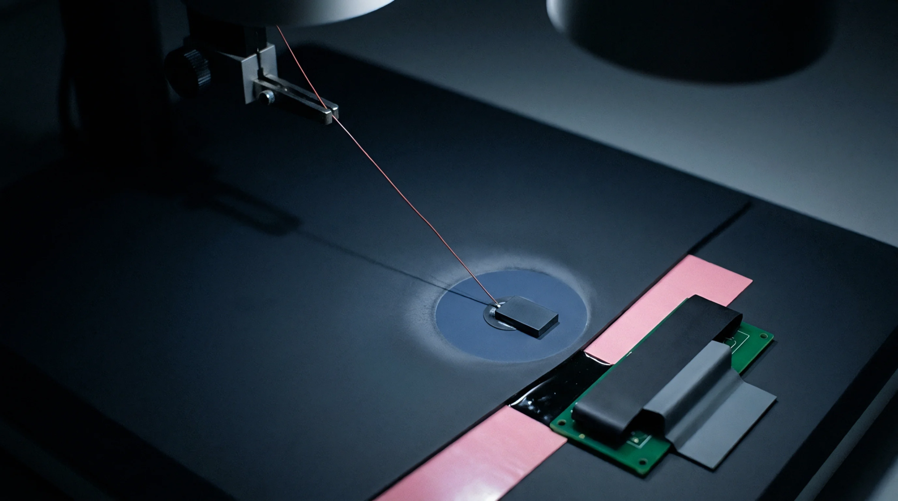
Measurement of the deviation utilizes a laser profiler to map the height differences relative to a flat reference surface. A board warping value is calculated as a percentage of the total length of the substrate.
Thermal Trigger
Heat exposure during the reflow soldering process often exacerbates latent stresses within the laminate. When the temperature crosses the glass transition point, board warping becomes more pronounced as the polymer matrix softens and resets. Differing densities of copper between the top and bottom layers create a bimetallic strip effect that forces the board into a curved shape.
Stiffening bars help. Proper control of cooling rates prevents secondary failures in solder joint integrity.
Acceptance Limit
The IPC-A-600 standard provides the primary guidelines for determining the maximum allowable bow and twist in finished boards. For surface mount technology, a maximum limit of 0.75 percent is common. These values are verified before the assembly stage begins.