Multi Point Temperature Sensor Integration for Sub Torr MEMS Resonator Drift Compensation
Spatial multi-point temperature sensing inside sub-Torr MEMS packages removes transient thermal gradient frequency drift down to sub-ppm precision limits.


Lag
In vacuum environments below 1 Torr, thermal transport across encapsulated cavities departs from fluid continuum behavior. When operating between 0.001 Torr and 0.1 Torr, gas molecules inside a microelectromechanical cavity have mean free paths substantially wider than the gap between the resonator beam and packaging cap. In the Knudsen regime (Knudsen numbers above 10), internal gas conduction falls by three orders of magnitude relative to atmospheric levels.
Heat transfer within the cavity collapses to solid-state conduction through silicon anchors and radiative exchange across micro-scale gaps.
This isolation creates a pronounced temporal lag between the external package enclosure and the resonant core. External thermal steps reach the ceramic frame and metal lid within tens of milliseconds, but the suspended silicon resonator mass exchanges heat almost entirely through its narrow mechanical anchors. Because those anchors are dimensioned for high quality factors to isolate acoustic and mechanical energy, they impose high thermal impedance.
That trade-off extends the thermal time constant to anywhere between 2 seconds and over 15 seconds, depending on anchor cross-section and substrate thickness.
0.01 Torr cavity pressure elevates resonator thermal time constants past 8 seconds.
A temperature sensor on the leadframe or the read-out ASIC registers transients immediately, while the resonator core responds much later. Relying on a single remote sensor for frequency-offset calibration produces substantial hysteresis during temperature ramps. Whenever ambient shifts exceed 0.05°C per second, the cap, anchor, and vibrating proof mass fall out of thermal equilibrium.
The resulting frequency error causes phase-locked loop tracking errors and timing instability in narrow-bandwidth communication applications.
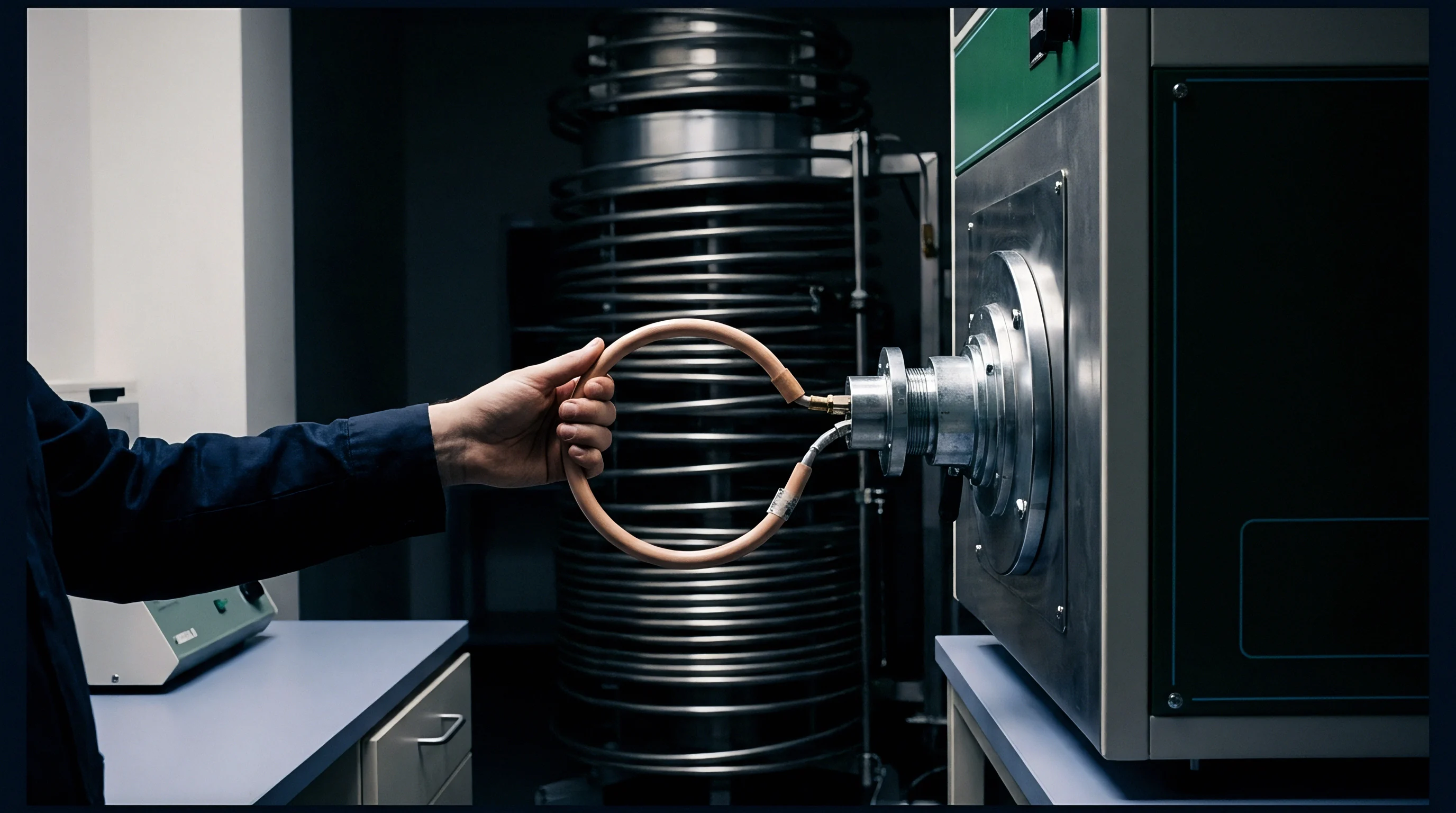
Rarefied Gas Conduction Limits
Sealed cavity pressure dictates the primary heat path. Near 760 Torr, molecular collisions govern thermal transport and keep internal structures closely coupled. Once getter activation pulls pressure below 0.1 Torr, molecule-to-wall collisions dominate over inter-molecular collisions.
Here, gas thermal conductivity scales directly with absolute pressure instead of holding constant as continuum theory assumes.
| Cavity Pressure Range | Dominant Heat Transfer Path | Thermal Time Constant Range | Primary Thermal Impedance Source |
|---|---|---|---|
| 760 Torr to 10 Torr | Fluid Convection and Gas Conduction | 10 ms to 100 ms | Boundary Layer Air Resistance |
| 10 Torr to 0.1 Torr | Transition Regime Gas Conduction | 100 ms to 1.5 s | Rarefied Molecular Gas Gap |
| 0.01 Torr to 0.0001 Torr | Solid Anchor Conduction and Radiation | 2.0 s to 18.0 s | Silicon Anchor Beam Geometry |
Sub-micron radiative heat transfer follows the Stefan-Boltzmann relationship, weighted by the emissivity of doped silicon and metal layers. Between -40°C and 105°C, radiation accounts for less than 5 percent of total heat flux; silicon anchors remain the only meaningful thermal path. Thermal models predicated on atmospheric coupling therefore fail to capture dynamic frequency excursions during thermal shock events.

Solid Anchor Conductive Coupling
Support beams are engineered to minimize energy loss into the package substrate, with narrow geometries pushing quality factors past 100,000 in disk and tuning-fork topologies. Heat flux through the silicon beam follows Fourier conduction, scaling with cross-sectional area and thermal conductivity and inversely with length. Silicon conductivity falls from roughly 148 W/(m·K) at 25°C to under 100 W/(m·K) at 125°C, which compounds lag at elevated temperatures.
Temperature ramps drive heat from the substrate frame, through the anchor junction, and into the resonator body. Until diffusion stabilizes, thermal gradients across the vibrating element remain uneven. Evaluating frequency stability without accounting for spatial anchor differentials leads to severe timing jitter under real-world operating profiles, and ignoring this time-constant mismatch in sub-Torr cavities causes phase-locked loop unlocking during industrial heat spikes.


Array
Resolving dynamic gradients in vacuum packaging requires distributed sensing at critical structural nodes. Placing sensors across the silicon substrate, anchor zones, and package lid creates a multi-point monitoring matrix that feeds spatial data to the compensation processor, distinguishing uniform ambient heating from directional ramps.
Localized sensing catches variations that single-point sensors blur together. Anchor points absorb heat from the substrate immediately, whereas the center of the vibrating beam lags. Symmetrically positioned sensor pairs around the anchor geometry enable differential extraction of directional gradients, preventing correction routines from overcompensating during rapid thermal swings.

What Spatial Gradient Limits High Precision Drift Compensation?
Gradients across the resonator alter local stiffness unevenly. Single-crystal silicon has a Young’s modulus temperature coefficient of roughly -60 ppm/°C. A 0.5°C gradient between anchor points on a double-ended tuning fork generates differential mechanical stress, shifting the natural resonance frequency independently of bulk expansion.
These gradients introduce higher-order cross-coupling into drift equations. While uniform heating shifts frequency according to static TCF1 and TCF2 coefficients, a dynamic gradient introduces stress-induced shifts proportional to the anchor differential. Without multi-node extraction, algorithms interpret stress-induced shifts as bulk drift, leaving residual errors above 5 ppm in sub-Torr timing units.
The unmitigated dynamic thermal errors manifest in predictable operational modes across the sensor lifetime:
- Anchor Differential Lag creates transient frequency spikes during directional packaging heat flux events.
- Lid to Substrate Offset induces radiative heat asymmetry across upper and lower surface profiles.
- ASIC Heat Dissipation generates localized planar thermal gradients across adjacent die mounting zones.
- Stress-Induced Modulus Shift perturbs high-Q mechanical resonance modes outside predicted calibration curves.

Sensor Geometry and Placement Metrics
Sensor placement balances sensitivity against routing complexity and die area. Diodes embedded directly in the anchor substrate respond fastest to incoming substrate heat flux. A quad-point layout, with sensors in each quadrant of a square die, provides full three-dimensional surface mapping.
Cap-mounted sensors detect external shifts before heat reaches the internal die. Pairing three substrate sensors with one cap sensor separates external thermal inputs from internal dissipation. To maintain mathematical independence across readings, sensor spacing must exceed the die thermal diffusion length at the target sample rate.
Symmetrical anchor placement yields lower cross-axis thermal sensitivity than adding passive thermal shield masses.


Diode
Sensing elements in sub-Torr MEMS architectures must offer predictable voltage responses without imposing meaningful thermal or electrical loads. Common options include substrate p-n junction diodes, PNP transistors wired as diodes, and thin-film platinum RTDs. Forward-biased p-n junctions suit monolithic CMOS-MEMS integration well, providing a linear negative temperature coefficient of about -2.0 mV/°C at constant forward current.
Thin-film platinum RTDs on oxide passivation layers offer high stability and low hysteresis under thermal cycling, with a positive coefficient of roughly +0.00385 Ω/Ω/°C. However, platinum deposition requires non-standard CMOS foundry steps, whereas p-n junctions fit into standard silicon wells without additional masks.
Standard MIL-STD-883 Method 1010 Condition B specifies dwell times that force recalibration matrix verification across spatial equilibrium states.
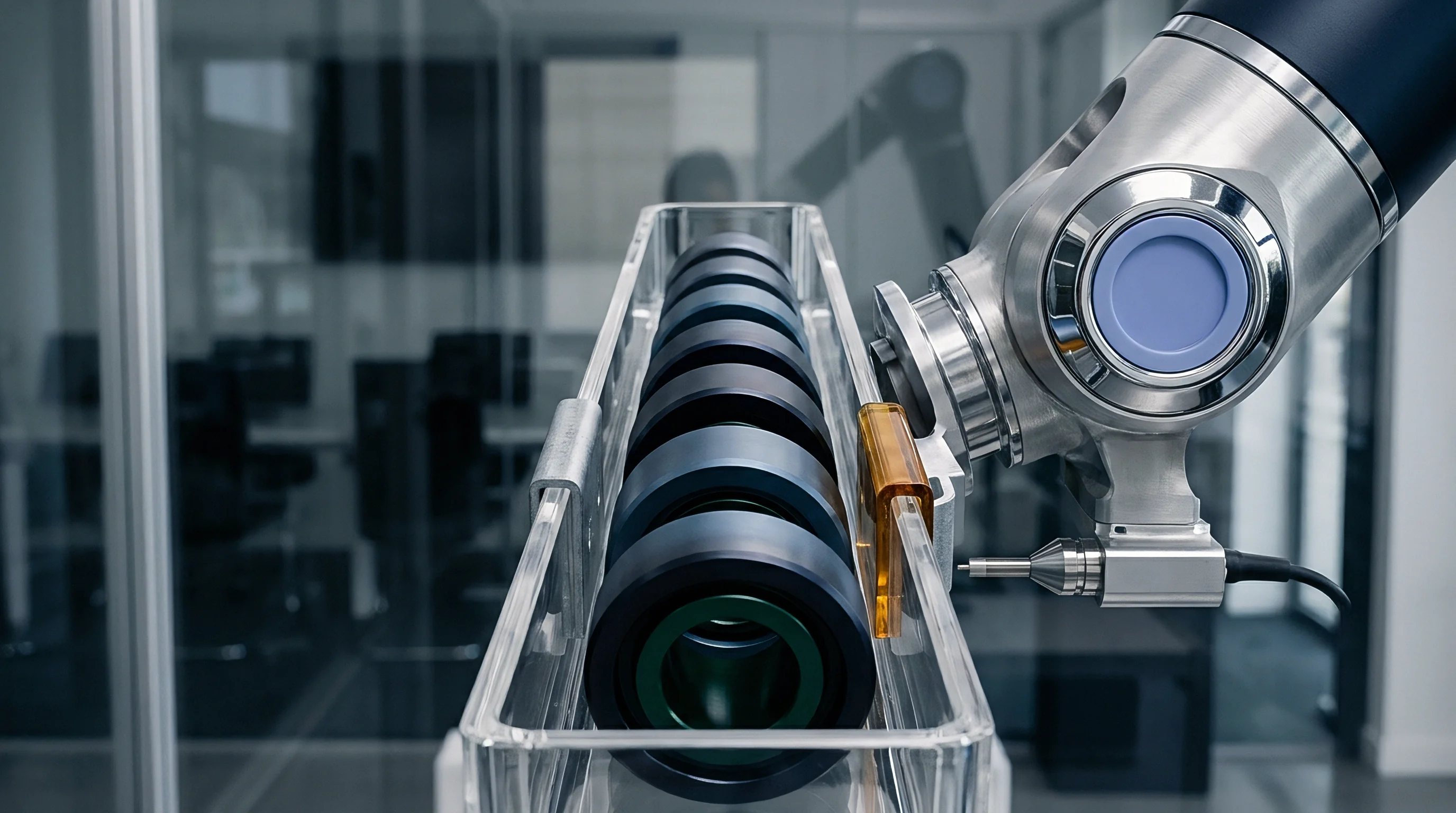
Integrated Substrate Transduction Mechanisms
Operating substrate PNP micro-diodes at two distinct current densities allows absolute temperature extraction via differential base-emitter voltage. Driving at a 10 to 1 ratio produces a voltage proportional to absolute temperature, scaled by the Boltzmann constant and electron charge. This PTAT measurement circumvents absolute forward-voltage tolerances tied to process variation and long-term doping drift.
Embedded diodes share the single-crystal silicon lattice with the flexures, reducing thermal interface resistance to near zero. Their thermal response bandwidth exceeds 1 kHz, capturing localized micro-heating transients that package-level sensors miss entirely.

Parasitic Self Heating and Drive Currents
Sensors in vacuum must operate at minimal power to prevent self-heating, since dissipated heat cannot escape through gas conduction. Thermal impedance from an embedded diode to the package base often exceeds 2,000 K/W. Running a diode at 100 µA with a 0.7 V drop dissipates 70 µW, raising local sensor temperature by 0.14°C above the surrounding silicon.
Pulsed or low-duty-cycle excitation keeps self-heating errors below 0.001°C. Driving diodes with 10 µA pulses at a 1 percent duty cycle cuts continuous dissipation to 70 nW. Front-end circuits sample the voltage within the pulse window before heating perturbs local equilibrium. Pulse durations must allow adequate settling without allowing heat to accumulate.
Lid temperature tracking die temperature closely does not eliminate the need for secondary thermal channels in high-reliability timing applications.


Matrix
Converting multi-node thermal data into frequency corrections requires spatial surface fitting. Where static single-point compensation uses standard Taylor series polynomials of temperature T, multi-point sub-Torr compensation employs a multidimensional matrix incorporating base temperature, planar gradients, vertical cap-to-substrate differentials, and time-derivative terms.
Mathematical modeling captures instantaneous frequency deviation using a spatial equation structure:
Δf / f₀ = A₀ + A₁(T_ref – T₀) + A₂(T_ref – T₀)² + B₁(ΔT_radial) + C₁(ΔT_axial) + D₁(dT_ref / dt)
The coefficients A₁ and A₂ account for linear and quadratic bulk temperature response, B₁ scales horizontal gradients across anchor pairs, C₁ compensates vertical differentials between the die and lid, and D₁ addresses transient lag via real-time rate derivatives.

Polynomial Gradient Surface Fitting
Extracting coefficients requires automated multi-axis calibration in environmental chambers. Assemblies are cycled across their operating range under dynamic thermal ramps between 0.1°C per minute and 10°C per minute, recording output frequency alongside synchronized sensor voltages.
Least-squares matrix inversion calculates polynomial coefficients for each assembly. Storing these parameters in on-chip EEPROM or flash memory allows internal DSP blocks to apply continuous real-time corrections, pulling dynamic frequency excursions down to sub-ppm levels under thermal shock.

Worked Scenario Thermal Ramp Verification
A 32 MHz silicon micro-resonator in a 0.005 Torr package subjected to a 2.0°C per minute ramp from 25°C to 85°C exhibits an uncompensated frequency shift of -1800 ppm across the 60°C span, based on a primary temperature coefficient TCF1 of -30 ppm/°C.
Single-point compensation using a package-mounted sensor leaves lag errors. During a 2.0°C per minute ramp, high internal thermal impedance causes the silicon anchor to lag the package by 0.6°C, resulting in an uncompensated tracking error:
Error_dynamic = 0.6°C × 30 ppm/°C = 18.0 ppm
This 18.0 ppm error exceeds optical and wireless timing specifications, which routinely cap frequency tolerances at ±1.0 ppm under dynamic conditions.
A four-point sensing array (two anchor diodes, one cap sensor, and one ASIC reference diode) resolves these spatial differentials. At t = 15 minutes into the ramp, the array records:
T_anchor1 = 54.4°C, T_anchor2 = 54.2°C, T_cap = 55.0°C, T_asic = 55.2°C
The matrix processor calculates a bulk reference temperature T_ref = 54.3°C, radial anchor gradient ΔT_radial = 0.2°C, axial lid gradient ΔT_axial = -0.7°C, and rate derivative dT/dt = 0.033°C/s. Feeding these terms into the surface-fit model compensates both lag and stress components, bringing residual frequency error below 0.08 ppm across the ramp profile.
| Compensation Topology | Static Error Band (-40°C to 85°C) | Dynamic Error Band (1.0°C/min Ramp) | Dynamic Error Band (5.0°C/min Ramp) |
|---|---|---|---|
| Single-Point Uncompensated | ±1800 ppm | ±1850 ppm | ±1980 ppm |
| Single-Point Package RTD | ±0.5 ppm | ±8.5 ppm | ±38.0 ppm |
| Dual-Point Substrate Diode | ±0.2 ppm | ±1.2 ppm | ±4.5 ppm |
| Four-Point Matrix Array | ±0.05 ppm | ±0.08 ppm | ±0.25 ppm |
Accurate calibration requires a controlled factory procedure before shipment:
- Mount target oscillator assemblies onto low-thermal-mass test fixtures inside a temperature chamber with less than 0.05°C spatial variation.
- Stabilize environmental chamber at initial equilibrium baseline temperature of -40°C for 30 minutes.
- Apply continuous linear thermal ramp at 1.0°C per minute up to 105°C while logging frequency output and multi-point sensor voltages every 100 milliseconds.
- Perform multivariate least-squares matrix regression on captured thermal dataset to calculate individual die coefficient vectors.
- Burn calculated coefficient vectors into on-chip non-volatile memory registers and execute secondary verification sweep.
Dynamic thermal gradient compensation performance maps directly to spatial sensor resolution and matrix fit accuracy.
Section 4.2 of standard IEEE 1158 requires frequency stability metrics under dynamic environmental thermal ramps to state spatial sensor thermal time constants explicitly.


Conversion
Resolving microvolt-level sensor shifts without injecting noise is essential for sub-ppm compensation. With a p-n diode sensitivity of -2.0 mV/°C, resolving 0.001°C requires detecting 2 microvolts. Differential noise across the analog-to-digital converter path must stay comfortably below this 2 microvolt threshold across the conversion bandwidth.
Continuous-time delta-sigma ADCs with high-order sinc filters are well suited to multi-point thermal acquisition. High oversampling ratios and noise shaping push quantization noise into upper frequencies, where digital decimation filters remove it. A 24-bit delta-sigma converter running between 10 Hz and 100 Hz delivers noise-free resolution above 20 bits.

Delta Sigma Resolution and Filtering
Analog front-ends require low-noise instrumentation amplifiers and stable voltage references. Reference drift directly degrades conversion accuracy: a 10 ppm/°C reference shift mimics sensor drift and corrupts frequency compensation. Active thermal trimming on bandgap references holds drift below 0.5 ppm/°C over industrial temperature spans.
Decimation filtering must balance 50Hz/60Hz mains rejection against group delay. Excessive filter latency introduces phase lag into the correction loop, undermining performance during fast ramps. Sinc3 and sinc4 filters configured for a 20 Hz data rate offer a practical compromise between noise rejection and phase delay.

Multiplexing Latency and Noise Floors
Multiplexing several sensors through a single ADC introduces inter-channel delays. Sampling four sensors with a 50 millisecond delay per channel requires 200 milliseconds per complete sweep, introducing skew that appears as artificial spatial gradients during fast ramps.
Simultaneous-sampling architectures using dedicated delta-sigma modulators per channel eliminate this skew. Although dedicated channels increase die area and current draw, they preserve synchronization across all measurement points. For low-power sub-Torr timing, duty-cycled simultaneous sampling outperforms high-speed sequential multiplexing during dynamic tracking.
Whether dynamic chopping in delta-sigma converters can fully eliminate low-frequency flicker noise without introducing thermal switching crosstalk into the resonator core remains open for sub-ppm oscillators.


Supply
Sourcing multi-point compensated MEMS timing devices involves assessing foundry integration, packaging flows, and component longevity. Monolithic CMOS-MEMS combines the resonator, diode array, analog front-end, and matrix processor on a single die, whereas dual-die co-packaging houses a MEMS die alongside a dedicated ASIC inside one hermetic package.
Monolithic integration eliminates bond-wire parasitics and minimizes thermal time constants between sensors and the resonator, but demands specialized processes combining high-aspect-ratio etching with CMOS fabrication. Dual-die packaging allows the MEMS and ASIC processes to be optimized independently, broadening commercial foundry options.

CMOS MEMS Foundry Packaging Integration
Sub-Torr packaging uses ceramic leadless chip carriers sealed with gold-tin eutectic preforms or glass frit bonding. Alternatively, wafer-level encapsulation builds micro-cavities across the wafer by bonding silicon caps directly to device wafers, cutting component footprint to chip-scale dimensions while maintaining pressures below 0.01 Torr over 15-year lifespans.
Packaging substrates dictate mechanical stability and outgassing performance. Low-temperature co-fired ceramic provides matched thermal expansion relative to silicon, curbing assembly stress. Because adhesive outgassing degrades sub-Torr vacuum levels over time, inorganic die-attach materials or gold-silicon eutectic bonding are needed to preserve cavity pressure and thermal transfer characteristics.

Dossier Criteria for Sourcing Desk Verification
Sourcing dossiers for high-reliability sub-Torr oscillators require verification of qualification metrics. Package integrity and sensor accuracy must be confirmed through test documentation before approving production suppliers.
Sourcing desks should enforce a rigid qualification checklist during vendor audits:
- Hermeticity Verification Testing confirms helium fine-leak rates remain below 1×10⁻⁹ atm·cm³/s per MIL-STD-883 Method 1014.
- Getter Capacity Documentation validates reactive metallic getter film thickness is sufficient to absorb outgassed hydrogen and water vapor across storage lifetimes.
- AEC-Q100 Grade 0 Qualification proves operational stability from -40°C to 150°C under severe vibration and thermal stress profiles.
- Multi-Point Sensor Calibration Reports demonstrate individual sensor linearity and absolute accuracy across entire dynamic operating ranges.
- Thermal Cycling Hysteresis Limits verify residual frequency offset stays below ±0.1 ppm after 1,000 thermal shock cycles.
Multi-sourcing agreements require confirming that secondary ASIC foundries can consume identical matrix calibration formats without software modifications. Dual-sourcing mitigates allocation risk when foundry capacity tightens across advanced MEMS packaging lines.