Silicon Substrate Stress Isolation in Micro Inertial Packages
Substrate stress isolation protects micro inertial die from packaging strain through balanced micro-machined anchors and compliant low-modulus die-attach layers.

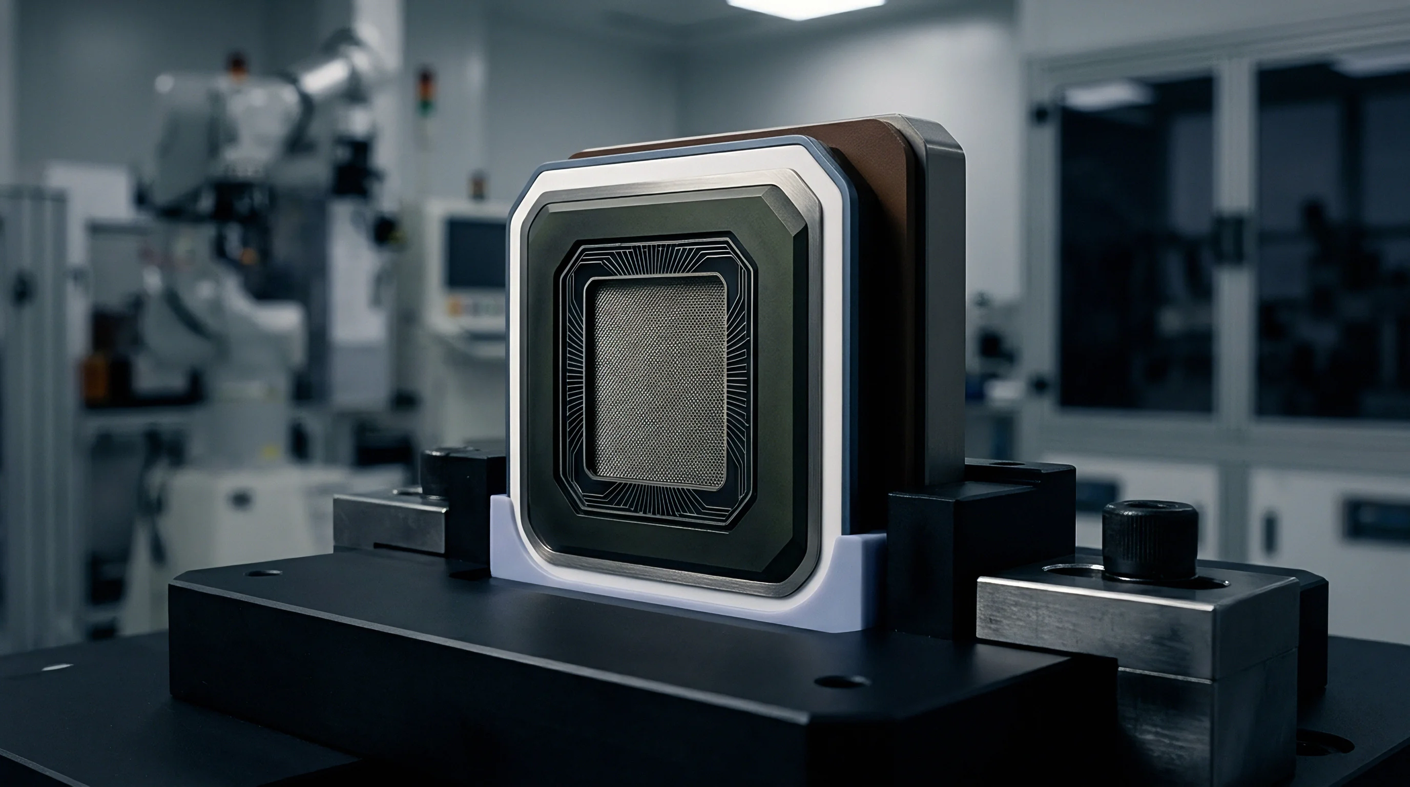
Gradient
Mechanical loads transferred through an inertial sensor package disturb the equilibrium of internal micromachined suspensions. As external forces pass through circuit board traces, solder joints, and plastic encapsulants, the underlying silicon substrate deforms. This strain shifts the baseline position of comb fingers in differential capacitive accelerometers, generating false acceleration signals.
In tuning fork gyroscopes, package stresses alter the drive and sense resonant frequencies independently, widening the frequency split and degrading quadrature rejection. At sub-angstrom scales, these structural distortions produce signals identical to genuine physical motion.
Interfacial shear between printed circuit assemblies and component packages stems from thermal expansion mismatches. FR4 substrate expands laterally at 14 to 17 parts per million per Kelvin, whereas single-crystal silicon expands at only 2.6 parts per million per Kelvin. Cooling from the 260 degrees Celsius peak reflow temperature down to room ambient leaves a surface-mount sensor in a continuous compressive state.
Asymmetric copper traces beneath the footprint add directional bending moments that flex the package body. As operating temperatures cycle between minus 40 degrees Celsius and 125 degrees Celsius, these thermal-mechanical forces generate dynamic load vectors across the die attach boundary.
Under an applied bending field of 500 microstrain, an unisolated capacitive sensing cavity exhibits a 14 milligram zero-g offset drift across a 60 Kelvin thermal transition.
Substrate flexure triggers several distinct physical failure modes within micro-electro-mechanical sensor structures:
- Capacitive gap shrinkage alters sense capacitance by fractions of a femtofarad, directly corrupting the primary voltage conversion stage.
- Resonance splitting distortion shifts the mechanical sense channel away from the electrostatic drive frequency, inducing phase noise in the rate demodulator.
- Anchor point rotation tilts comb tooth structures out of their nominal parallel planes, degrading common-mode electrostatic cancellation.
- Piezoresistive bridge unbalance shifts zero-measurand output voltages in bulk micromachined elements through localized crystallographic lattice compression.

Thermoelastic Board Deflection Mechanics
Board warping forces enter the package directly through solder interconnects. Quad flat no-lead assemblies transfer bending moments through corner solder fillets into the ceramic or molded housing. Ball grid arrays distribute these forces across outer solder spheres, translating board curvature into vertical peeling stresses at the die edge.
Finite element modeling indicates that a 1-millimeter board deflection across a 100-millimeter span imposes up to 45 megapascals of tensile stress on a silicon die bonded directly to the cavity floor.
Once transmitted through the package floor, this stress propagates directly into the delicate internal suspension.
Crystalline orientation governs how silicon responds to these boundary loads. Wafers etched along the (100) plane exhibit anisotropic elasticity, with Young’s modulus shifting from 130 gigapascals along the axis to 169 gigapascals along the axis. Bending loads aligned with crystal directions produce uneven strain profiles across perpendicular suspension flexures.
This structural asymmetry creates parasitic cross-axis sensitivity, converting planar inputs into spurious out-of-plane proof mass displacement.

Piezoelectric and Piezoresistive Bias Induction
Doped silicon sense resistors alter their values linearly with strain through the piezoresistive effect. In p-type silicon, longitudinal and transverse piezoresistive coefficients reach 71.8 and minus 66.3 times ten to the negative eleven square meters per newton along the direction. Packaging strain reaching the silicon bulk alters the offset of balanced Wheatstone bridges, producing a calibration drift that the signal chain cannot distinguish from genuine physical acceleration.
As thermal or mechanical forces flex the package frame, the inner cavity distorts accordingly.
This distortion causes capacitive sensing gaps to narrow unevenly across the array.
Differential capacitive readouts also suffer secondary disruptions from altered squeeze-film damping and gap permittivity. When package strain reduces the nominal 1.2-micrometer gap between stator and rotor fingers by just 20 nanometers, electrostatic spring softening shifts the resonant frequency by several percent. In open-loop rate sensors, this geometric change degrades scale factor linearity, causing navigation drift that grows quadratically over time.
Without effective strain isolation at the die attach, factory calibration offsets drift over time, ultimately leading to field failures in high-precision navigation hardware.


Anchor
Isolating the sensing elements from package distortion requires dedicated strain-relief structures built directly into the silicon. Rather than bonding the entire die underside to the package cavity, micromachined isolation features separate active elements from external stresses. Suspending the functional frame on internal silicon flexures or anchoring it to a single central post allows the outer boundary to absorb package strains without warping the internal sensor geometry.
Without decoupling, asymmetrical strain tilting the proof mass introduces severe zero-g offset errors.
Central pedestal designs isolate the sensing core by anchoring the die to the package floor exclusively through a single central junction. Outer portions of the die remain suspended over an etched cavity, enabling the package underneath to flex without imparting shear stress to the active frame. This configuration cuts package-induced stress in the sensing zone by more than a factor of 20 compared to conventional full-backside bonding.
Deep reactive-ion etching forms these geometries in silicon-on-insulator wafers, creating narrow isolation channels around accelerometer and gyroscope cores.
Isolation efficiency increases as the mechanical compliance of the suspension spring exceeds the stiffness of the active sensing frame.
Designing effective silicon isolation requires balancing several interrelated geometric and mechanical factors:
- Flexure beam width controls spring compliance, balancing shock survival against decoupling efficiency along active axes.
- Isolation trench depth defines the vertical clearance required to prevent mechanical stiction against the lower package carrier.
- Central post area determines adhesive contact resistance and sets the lower frequency limit for parasitic packaging rocking modes.
- Crystallographic orientation alignment minimizes anisotropic stiffness divergence across multi-axis gyroscope suspension flexures.

Single Point Central Post Geometries
Creating central anchor structures relies on silicon-on-insulator processing with deep cavity etching. The functional layer, typically 20 to 50 micrometers thick, sits above a handle wafer separated by a buried oxide layer. Backside micromachining clears material from around the central region, leaving a single supporting boss under the center of mass.
As surrounding package materials expand or contract, the unbonded peripheral silicon moves freely without distorting the sense combs.
Because single-crystal silicon cleaves along crisp crystallographic planes, precise mask alignment is essential during anchor etching.
Parasitic resonance represents the main vulnerability of single-point anchor systems. Supporting the die on a small central post lowers the structural resonance into typical operating vibration bands. If the anchor lacks sufficient torsional stiffness, rocking modes can appear below 2 kilohertz, where environmental vibration excites the die mass and causes severe signal clipping or rectification.
To prevent this, designers stiffen the central boss while thinning the surrounding isolation beams, pushing parasitic modes above 10 kilohertz and out of the operational frequency band.

Suspended Silicon Interposer Isolation Layers
Micromachined interposers act as a mechanical buffer between the package base and the sensing die. Here, the sensor die attaches to a dedicated silicon carrier patterned with serpentine spring beams, which in turn mounts to the ceramic or laminate package using standard die-attach processes. Stresses from reflow soldering and thermal cycling are absorbed by the elastic compliance of the interposer beams before reaching the primary die.
External mounting assembly clamping forces can also deform the package leadframe, making decoupling essential.
| Architecture Scheme | Stress Reduction Ratio | Resonant Frequency Drop | Shock Tolerance at 0.5 ms | Silicon Area Penalty |
|---|---|---|---|---|
| Solid Full Die Attach | 1.0 | 0 percent | 10000 g | 0 percent |
| Perimeter Beam Frame | 4.2 | 12 percent | 5000 g | 18 percent |
| Central Pedestal Anchor | 22.5 | 35 percent | 2500 g | 8 percent |
| Suspended Silicon Interposer | 45.0 | 48 percent | 1500 g | 65 percent |
Increasing suspension compliance improves zero-g offset stability across temperature, but reduces the sensor’s ability to survive heavy mechanical shock.

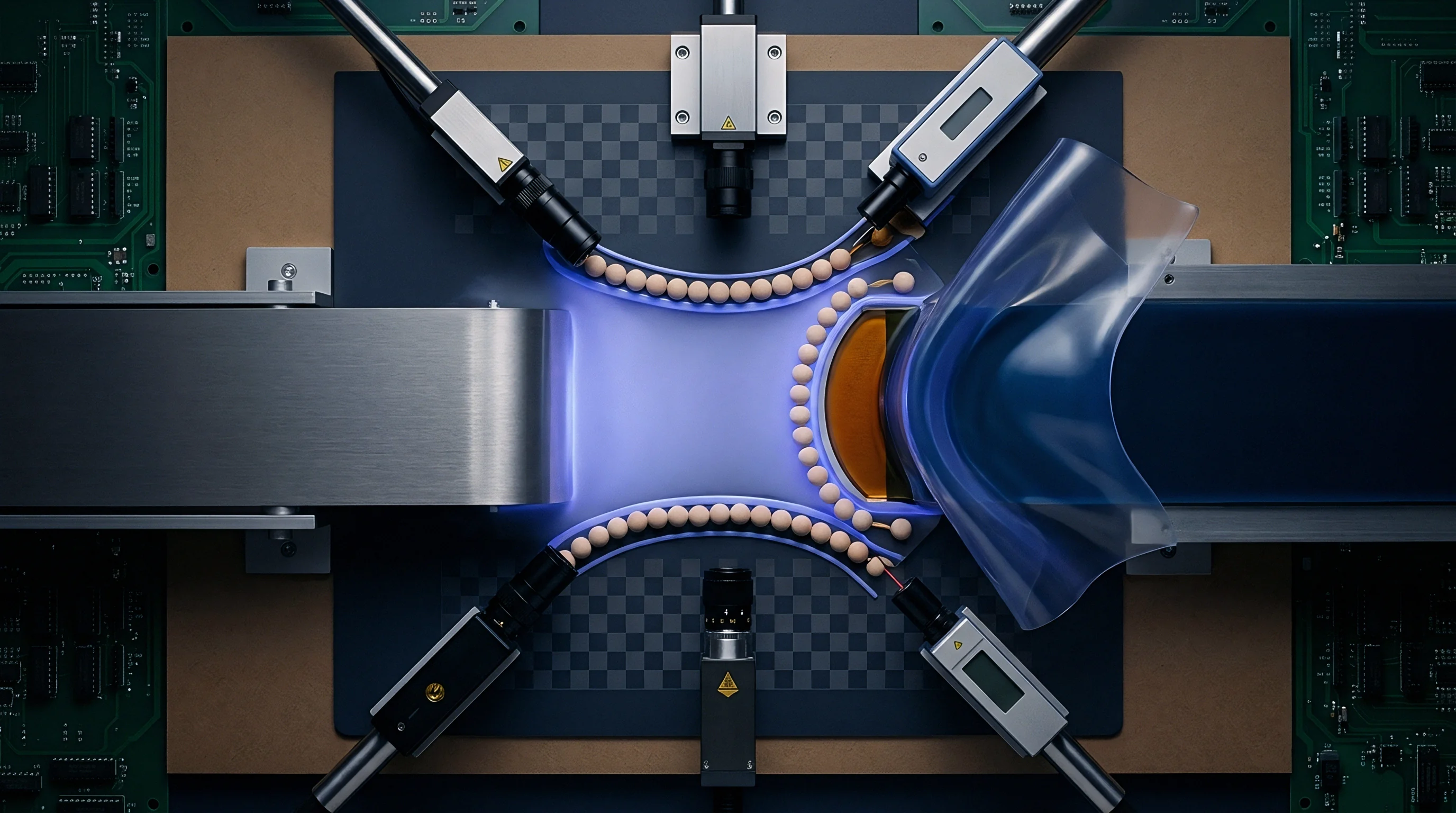
Resin
Polymeric die-attach materials dictate how stress transfers from the package carrier into the silicon die. The mechanical properties of these adhesives determine whether structural deformations pass directly into the substrate or cushion within the bondline. Formulations combine epoxy, silicone, or polyimide bases with conductive metallic or mineral fillers to trade off mechanical compliance, thermal conductivity, and electrical grounding performance.
As thermosetting epoxies cure, volume shrinkage creates baseline curing stress across the die footprint.
The glass transition temperature (Tg) marks a major shift in adhesive properties. Below Tg, the polymer remains rigid, with storage moduli between 1 and 10 gigapascals. Above Tg, molecular mobility increases and the material softens into a rubbery state, with storage moduli dropping below 10 megapascals.
When a sensor operates across an automotive range from minus 40 degrees Celsius to 125 degrees Celsius using an adhesive with a Tg near 50 degrees Celsius, its boundary stiffness changes by two orders of magnitude mid-range, producing pronounced non-linear bias shifts.
A compliant silicone die attach with an elastic modulus below 5 megapascals attenuates board flexure strain transmission by 85 percent compared to standard conductive epoxy.
Quality inspection routines evaluate polymer adhesives against several critical physical benchmarks:
- Storage modulus stability ensures consistent stress absorption across the operational temperature range.
- Bondline thickness uniformity prevents tilted die assemblies that induce asymmetric capacitive coupling.
- Outgassing condensable volatility must register below 0.1 percent to prevent contaminant condensation on open comb fingers.
- Moisture absorption coefficient determines susceptibility to hygroscopic swelling and long-term zero-bias wander.

Viscoelastic Modulus across Temperature Regimes
Silicone die-attach formulations offer stable compliance over wide operating ranges. Because their glass transition lies below minus 100 degrees Celsius, silicones maintain a low modulus of 1 to 5 megapascals from minus 60 degrees Celsius to over 200 degrees Celsius. Thermal stresses caused by CTE mismatches dissipate through viscoelastic relaxation in the matrix, leaving the sensor die largely isolated on a compliant cushion.
When temperatures drop below the transition point, polymer chains lock into place, abruptly increasing stress coupling.
Soft adhesives complicate wire bonding and die placement. During thermosonic wire bonding at 150 to 180 degrees Celsius, a compliant bondline absorbs ultrasonic energy, causing non-stick failures on bonding pads. Manufacturing lines address this by adjusting ultrasonic power, switching to epoxies engineered for low-temperature flexibility, or using dual-cure materials that remain rigid during wire bonding and soften during final cure.
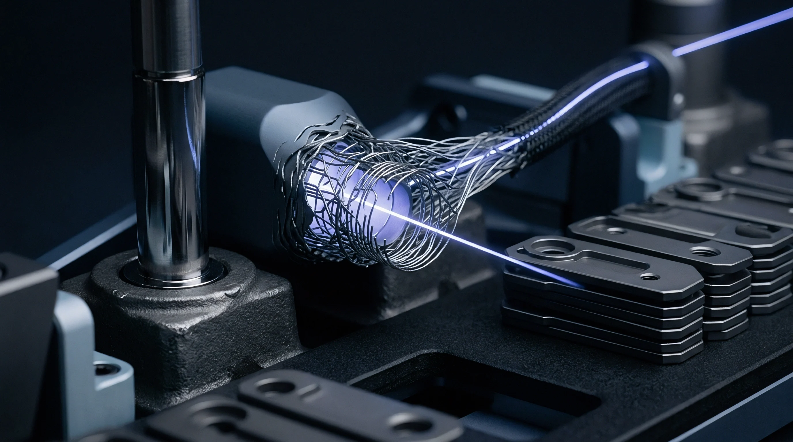
Void Formation and Warpage Asymmetry
Voids inside the die-attach layer disrupt strain symmetry across the die backing. Solvent evaporation and outgassing during cure can leave empty pockets under the silicon. A void beneath one quadrant interrupts uniform stress distribution, causing unsupported areas to remain stress-free during temperature swings while adjacent bonded regions experience full CTE expansion forces.
Extreme local warpage gradients can concentrate stresses near wire bond footprints, leading to mechanical fatigue.
| Material Class | Elastic Modulus at 25 C | Glass Transition (Tg) | CTE Below Tg | Die Shear Strength at 25 C |
|---|---|---|---|---|
| Silver-Filled Epoxy | 6500 MPa | 120 C | 45 ppm/K | 22 MPa |
| Modified Flexible Epoxy | 450 MPa | minus 15 C | 110 ppm/K | 12 MPa |
| Polymerizing Silicone | 3.5 MPa | minus 115 C | 320 ppm/K | 4 MPa |
| Gold-Tin (80/20) Eutectic | 59000 MPa | 280 C (Melting) | 16 ppm/K | 150 MPa |
Minor bondline voids exert negligible effect on gross die shear strength under military standard limits, yet localized stress imbalances still induce significant offset drift in precision sensing cavities.
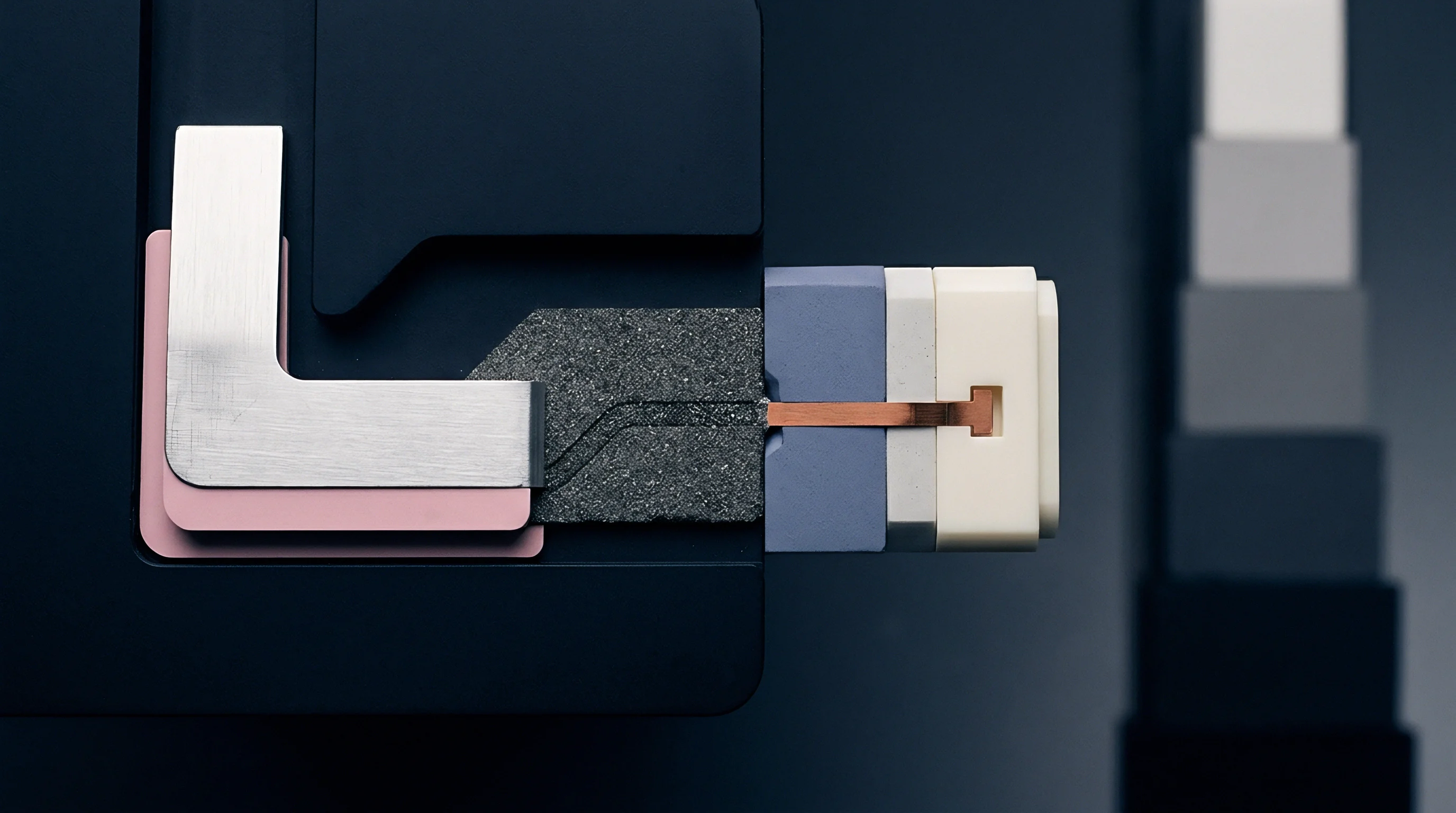
Hysteresis
Thermo-mechanical hysteresis degrades sensor calibration after thermal cycling. As an inertial package traverses hot and cold extremes, internal stress paths do not return along their original curves. Micro-scale slip in die-attach polymers, work hardening in metal leadframes, and viscoelastic relaxation in mold compounds retain residual stress in the package assembly.
When returning to 25 degrees Celsius, the die remains under altered baseline strain, which the signal path registers as permanent offset shift or rate drift.
Differing expansion rates across package layers force continuous structural bowing during thermal transitions.
As these internal stress states evolve, the sensor’s zero-g offset shifts unpredictably.
Solder joint metallurgy plays a major role in non-recoverable mechanical hysteresis. Common lead-free alloys like tin-silver-copper (SAC305) operate at roughly 60 percent of their melting point at 25 degrees Celsius, keeping them well within their active creep regime under normal room conditions. Strains from board bending or thermal cycles relax via grain boundary sliding and dislocation movement within the solder joints, permanently shifting the force balance between board and package.
A surface-mount package exposed to three thermal cycles from minus 40 degrees Celsius to 125 degrees Celsius experiences up to 80 milligram irreversible zero-g bias shift due to solder matrix work hardening.
Soldering Thermal Excursions and Zero Bias
Surface-mount reflow subjects devices to severe thermal shock, reaching temperatures above 250 degrees Celsius for 30 to 60 seconds. Differential contraction during cooling establishes the component’s baseline residual stress state. Plastic mold compounds shrink between 0.2 and 0.8 percent as they cool and complete post-mold curing; ceramic packages avoid mold shrinkage but pass solder solidification stresses directly into cavity walls.
While solder creep gradually relieves initial shear forces, it introduces long-term positional drift.
Once the assembly cools completely, these unaligned residual strains remain locked within the package structure.
Factory calibration performed before surface mounting often changes during reflow assembly. Although surface tension centers the package on its pads, uneven cooling locks asymmetrical strain fields into opposite corners. Precision IMUs require system calibration after board assembly to correct these baseline shifts, though post-assembly calibration cannot prevent subsequent drift caused by solder aging and mechanical vibration over time.
Mechanical Relaxation in Solder Joint Stacks
Intermetallic growth creates ongoing drift mechanisms in surface-mount assemblies. Copper from PCB pads diffuses into tin-rich solder, forming brittle Cu6Sn5 and Cu3Sn intermetallic layers along the joint interface. These intermetallics feature high elastic moduli above 110 gigapascals and do not yield plastically under stress.
As intermetallic layers thicken over extended field operation, perimeter joint stiffness becomes increasingly asymmetrical, causing continuous zero-point calibration drift.
As solder joints undergo continuous stress relaxation, the package strain profile continues to evolve indefinitely.
| Package Construction | Hermetic Cavity | Residual Stress Level | Zero-g Thermal Hysteresis | Gyro Bias Stability (Allan Dev) |
|---|---|---|---|---|
| Plastic Molded QFN | No | 35 to 80 MPa | 15.0 mg | 8.5 deg/hr |
| Ceramic LCC Cavity | Yes | 10 to 25 MPa | 3.5 mg | 1.2 deg/hr |
| Ceramic with Interposer | Yes | 1 to 5 MPa | 0.4 mg | 0.08 deg/hr |
| Metal Can Header | Yes | 0.5 to 2 MPa | 0.1 mg | 0.02 deg/hr |
Eliminating intermetallic growth in lead-free solder joints remains an ongoing metallurgical challenge in high-reliability sensor design.


Screening
Quality assurance protocols need to verify that stress isolation structures function properly after board assembly. Standard automated test equipment reads electrical parameters at room temperature, which masks strain sensitivity. Comprehensive qualification requires active board-level deflection testing while monitoring device output in real time, using mechanical actuators to apply controlled strain steps while tracking bias drift.
Standard four-point bend testing following IPC-9704 guidelines evaluates this sensitivity under controlled deflection. Test vehicles instrumented with strain gauges undergo cyclic mechanical bending while attached sensors stream output data. The ratio of sensor output shift to applied microstrain yields the package stress rejection factor.
Industrial sensors typically maintain shifts below 0.05 milligrams per 1000 microstrain, whereas consumer-grade components frequently exceed 2.5 milligrams under identical loading.

Four Point Bend Testing Methods
Cyclic bend testing separates elastic isolation efficiency from plastic hysteretic effects. Fixtures hold a standard 1.6-millimeter FR4 board between outer anvils spaced 100 millimeters apart, applying loads through two inner rollers. Stepper motors generate cyclic strains up to 2000 microstrain at frequencies from 0.1 to 10 hertz.
Signal processing with lock-in amplifiers tied to the drive actuator separates strain-induced output shifts from background sensor noise.
Piezoresistive test dice can map local strain fields across the die surface during mechanical testing. On-chip resistor rosettes near die corners and center points allow direct measurement of normal stresses sigma-xx and sigma-yy as well as in-plane shear stress tau-xy. This empirical mapping validates finite element models and highlights subtle bending moments caused by asymmetric board routing.
Temperature Cycle Dwell Impact
Environmental qualification defines the limits of compliant die-attach materials under thermal stress. Standard protocols specify thermal shock and temperature cycling intervals with defined dwell times. For AEC-Q100 Grade 1 qualification, components undergo 1000 thermal cycles between minus 40 degrees Celsius and 125 degrees Celsius, with mechanical integrity evaluated by comparing pre-test and post-test calibration profiles.
Under AEC-Q104 paragraph 4.2, board-level reliability testing combines post-assembly thermal cycling with mechanical vibration to verify component durability for automotive applications.