Thin Film Strain Gauge Sputtering Process Basics
Direct magnetron sputtering of nickel-chromium alloy onto insulated substrates produces strain gauges with sub-micron thickness, zero glue creep, and low thermal drift.


Plasma
Generating a high-density glow discharge inside a high-vacuum chamber requires precise balance between ionization energy and gas throughput. Physical vapor deposition for strain sensing relies on accelerating noble gas ions toward a solid metallic target inside an evacuated vessel. Argon serves as the standard process gas due to its inert atomic structure and heavy mass, which matches common transition metals used in piezoresistive grid patterns.
Base pressures prior to processing set the baseline contamination level. Chamber pump-down to below 1.0 x 10^-4 Pa eliminates residual water vapor and oxygen molecules that alter film resistivity. When high vacuum is achieved, argon gas enters through mass flow controllers to elevate working pressures to operational levels.

Working Pressure Windows and Ion Density
Maintaining gas levels between 0.1 Pa and 1.0 Pa establishes the mean free path necessary for ejected metal atoms to reach the substrate. Excessively high pressure causes gas-phase scattering, reducing kinetic energy at impact and creating porous film structures. Pressure set too low extinguishes the electrical discharge.
Target excitation relies on direct current power for conductive metal alloys, while radio frequency power drives non-conductive ceramic dielectric targets. Direct current excitation supplies continuous negative bias to the target face, pulling positive argon ions from the ionized gas plume at high velocity. Energetic ion impact knocks target atoms free through momentum transfer across the cathode sheath.
Argon gas ions strike the cathode. Ejected atoms traverse the vacuum gap. Substrate positioning controls deposition uniformity across the batch.
A bias voltage shift from negative 50 to negative 100 volts alters target sputtering yield by eighteen percent at 0.5 Pa argon pressure.

Magnetron Confinement Mechanics for Thin Sensor Foils
Crossed electric and magnetic fields trap electrons near the cathode face, increasing collision probability by orders of magnitude. Permanent rare-earth magnets positioned behind the sputtering target form closed magnetic loops. Trapped electrons orbit along magnetic field lines above the target surface, producing dense localized ionization without raising bulk chamber temperatures.
Unconfined diode sputtering requires high gas pressures and elevated voltage, subjecting sensitive load cell bodies to damaging thermal radiation. Magnetron configurations concentrate energy directly into the erosion ring, maintaining substrate temperatures below 150°C during active deposition runs. Operating outside specified plasma power density boundaries causes target overheating, stoichiometry drift, and inconsistent film thickness across the sensor array.

Target
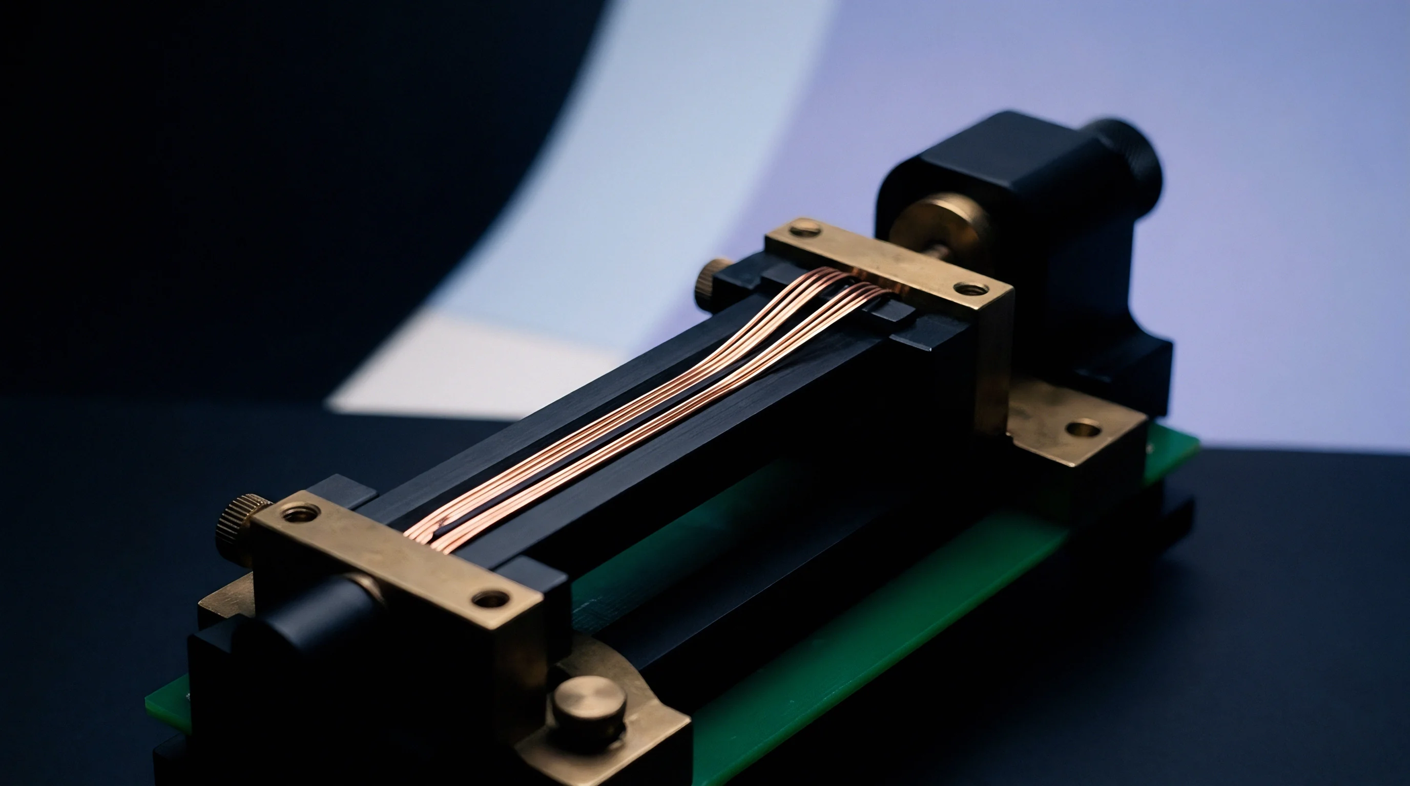
Raw material selection dictates the fundamental piezoresistive performance, thermal stability, and initial offset of the deposited sensing grid. Sputtering targets used in strain sensor production are vacuum-melted high-purity alloy discs or plates. Nickel-Chromium alloys containing 80 percent nickel and 20 percent chromium form the baseline material for general-purpose strain transducers due to their flat temperature response curve.
Purity grade selection directly influences electrical noise and signal stability. Targets produced to 99.99 percent purity contain trace iron, cobalt, and sulfur impurities that segregate to grain boundaries, acting as scattering sites for electrical charge carriers.

Stoichiometric Transfer in Binary and Ternary Alloys
Ejecting elements with differing atomic weights creates compositional shifts between the cathode surface and the deposited film. Nickel and chromium exhibit distinct sputtering yields under argon ion bombardment. Initial operational hours produce preferential ejection of the higher-yield constituent until a modified surface layer establishes steady-state equilibrium.
Target purity determines baseline noise. Stoichiometric shifts alter sensor resistance. Pre-sputtering against a movable shutter for thirty minutes stabilizes target surface chemistry prior to exposing cleaned substrate parts.
| Target Alloy Composition | Deposition Power Mode | Gauge Factor (GF) Range | Temperature Coefficient (ppm/°C) | Target Purity Standard |
|---|---|---|---|---|
| NiCr (80/20 wt%) | Direct Current (DC) | 2.0 to 2.2 | -10 to +20 | 99.99% |
| NiCrSi (75/20/5 wt%) | DC Magnetron | 2.1 to 2.3 | -5 to +5 | 99.995% |
| PtW (92/8 wt%) | RF Magnetron | 3.8 to 4.2 | +100 to +250 | 99.99% |
| TiN (Reactive Sputtered) | DC Reactive (Ar/N2) | 1.8 to 2.0 | -50 to -150 | 99.99% |
Purity Thresholds and Metallic Interlayers
Trace metallic contamination above fifty parts per million alters the temperature coefficient of resistance unpredictably. Modern sensor foundries specify triple-melt targets with gas-atomized powder compaction to guarantee isotropic composition across the entire erosion profile.
Adhesion promoting interlayers enhance structural bonding between insulating substrate layers and piezoresistive grids. Sputtering a thin titanium or chromium layer measuring 10 to 30 nanometers provides chemical bonding sites on oxide surfaces. Omitting this adhesion step results in delamination during cyclic mechanical loading, causing complete sensor open-circuit failures.
Sputtering equipment suppliers occasionally claim target composition shifts are self-correcting over time, but unconditioned target surfaces yield variable batch resistance values across early production runs.


Substrate
The physical base supporting the sensing film defines the mechanical load bearing capacity and dielectric isolation of the completed sensor. Load cell flexures machined from 17-4PH stainless steel, 316L stainless steel, or titanium alloys serve as primary structural substrates. Direct deposition onto metallic flexures eliminates organic adhesive interfaces, removing glue creep and mechanical hysteresis from the strain transfer path.
Substrate cleanliness dictates adhesion strength. Substrate surfaces require mechanical polishing to surface roughness values below 0.02 micrometers Ra. Microscopic peaks penetrating thin dielectric layers create electrical short-circuits to the metallic load cell body.

Dielectric Isolation and Surface Roughness Tolerances
Depositions executed directly onto conductive spring elements require an intermediate ceramic layer such as alumina or silicon dioxide. Radio frequency sputtering or reactive direct current sputtering deposits high-purity aluminum oxide films to thicknesses between 3 and 5 micrometers. This insulation barrier yields insulation resistance values exceeding 5 gigohms at 50 volts direct current bias.
Pinholes trigger electrical ground shorts. Dielectric breakdown destroys measurement integrity. Multi-layer insulation structures mitigate pinhole propagation through alternating deposition steps.
Substrate preparation and dielectric deposition follow strict physical guidelines to prevent sensor breakdown:
- Substrate Polishing Threshold ~ Diamond slurry lapping reduces metal flexure surface roughness to Ra 0.015 micrometers prior to solvent washing.
- Ultrasonic Degreasing Protocol ~ Sequential chemical baths in acetone, isopropyl alcohol, and deionized water remove organic oils and machining residues.
- In-Situ Plasma Etching ~ Reverse RF bias cleaning inside the vacuum chamber removes native oxide layers immediately before insulating film deposition.
- Dielectric Film Thickness ~ Alumina insulation thickness specified between 3.5 and 4.5 micrometers balances dielectric strength against thermal stress buildup.
- Insulation Breakdown Screening ~ High-voltage leakage testing subjects the dielectric layer to 100 volts DC before strain grid deposition begins.
Polishing load cell elements past the dielectric boundary roughness limit prevents micro-shunts across the insulating layer.

Thermal Expansion Mismatch and Interfacial Stress
Differing expansion rates between the metallic strain sensing film and the underlying body generate thermal stresses during temperature cycles. Grade 17-4PH steel possesses a coefficient of thermal expansion near 10.8 x 10^-6 /°C, whereas alumina insulation exhibits 7.2 x 10^-6 /°C, and NiCr film sits near 13.0 x 10^-6 /°C. Thermal stress alters baseline zero.
Cooling from deposition temperature induces interfacial shear stress proportional to layer thickness differences. Excessively thick ceramic insulation layers crack under severe thermal shock, destroying insulation resistance. Matching substrate prep methods to material coefficients ensures survival through operational thermal swings without delamination.


Lattice
Atomic arrangements within the deposited thin film determine electromechanical coupling, gauge factor stability, and long-term zero drift. As-deposited sputtered films exhibit fine-grained, highly disordered, or columnar microstructures containing high defect densities. Unstable crystal structures reorganize continuously over time at ambient temperatures, causing baseline resistance drift and unstable thermal expansion coefficients.
Resistivity varies with grain size. Post-deposition annealing drives crystal grain growth and defect annihilation. Subjecting sputtered sensing elements to vacuum or inert gas thermal treatment at 350°C to 450°C stabilizes the metallic lattice structure.

Post Deposition Thermal Stabilization Parameters
Subjecting freshly sputtered sensing grids to controlled heating cycles relieves residual stresses introduced during physical vapor deposition. Annealing shifts the temperature coefficient of resistance into a narrow band around zero ppm/°C. Unannealed NiCr films display negative TCR values due to high grain boundary electron scattering, shifting to positive values as grain coalescence occurs during heat treatment.
Thermal processing schedules dictate structural equilibrium. Heat treatment duration, peak temperature, and cooling rates are tightly regulated inside oxygen-free tubular furnaces.
| Annealing Temp (°C) | Atmosphere Condition | Dwell Time (Hours) | Post-TCR (ppm/°C) | 1000h Zero Drift (% FS) |
|---|---|---|---|---|
| 250 | Argon Gas Flow | 2.0 | -45 to -20 | 0.35% |
| 350 | High Vacuum (10^-3 Pa) | 4.0 | -5 to +5 | 0.04% |
| 420 | High Vacuum (10^-4 Pa) | 6.0 | -2 to +2 | 0.01% |
| 500 | Air Atmosphere | 1.0 | +30 to +80 | 0.85% |

Film Thickness Limits and Grain Growth Control
Deposition runs terminating between 50 nm and 250 nm yield optimum sensitivity while suppressing quantum size effects. Thinner layers under 30 nm show discontinuous island formation, leading to non-linear piezoresistive response curves. Layers thicker than 300 nm develop high internal stresses that induce film peeling.
Consider a worked construction evaluating a 100-nanometer NiCr strain gauge grid deposited on an alumina-insulated stainless steel load cell. The nominal bridge resistance measures 1000.0 ohms. Unannealed, the sensor displays a zero-point drift of 0.50 percent full scale per month under ambient storage conditions.
Subjecting the assembly to a vacuum anneal at 420°C for 6 hours reduces defect density by two orders of magnitude.
Following thermal stabilization, baseline drift drops to 0.01 percent full scale per year under continuous load cell excitation. The calculated Gauge Factor stays locked at 2.12 with non-linearity under 0.02 percent of full scale span. Micro-cracks degrade insulation resistance.
Direct deposition eliminates glue creep. Annealing sets crystal grain structure.
Compliance with ASTM E251 section 7 mandates zero-drift reporting across the full operating thermal range.
Contractual terms covering high-precision sensing elements reference specific test standards to govern batch qualification. Standard specifications mandate that supplier certificates include verified zero thermal shift coefficients and span drift limits measured across three full temperature cycles. Paragraph 4.2 of standard ISO/IEC 17025 governing calibration laboratory competence requires documenting uncertainty budgets for all environmental test chambers used during sensor qualification.

Verification
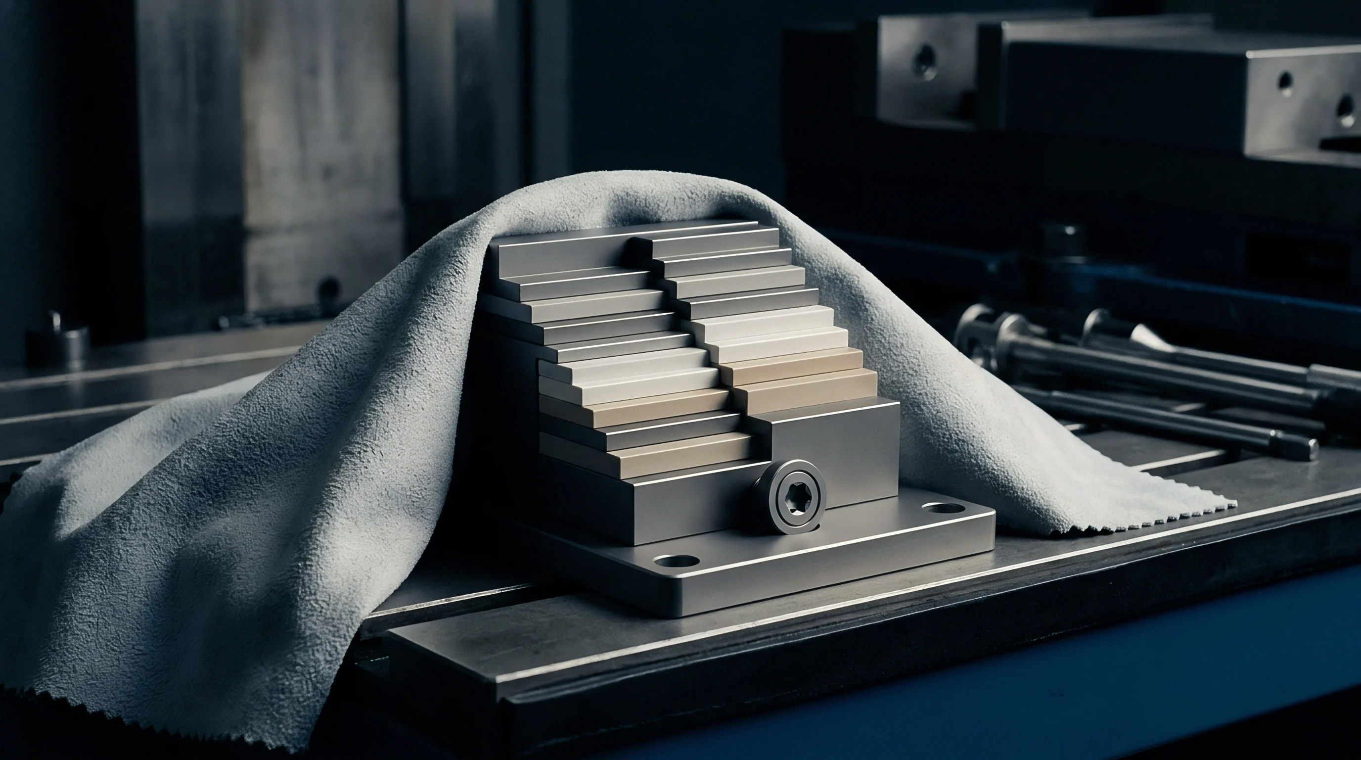
Accredited bench testing establishes whether a manufactured lot satisfies initial accuracy specifications and long-term stability limits. Metrologists verify piezoresistive performance using four-wire Kelvin resistance instruments coupled to temperature-controlled environmental chambers. Transducers undergo precise strain cycles applied by deadweight calibrator systems or precision bending beam fixtures traceable to national standards.
Bridge balance shifts over time. Oxygen contamination increases drift rates. Four-wire measurements isolate lead wire resistance from grid changes.

Uncertainty Budgets for Sputtered Strain Transducers
Combining individual error sources into an expanded statement requires evaluating Wheatstone bridge symmetry, excitation stability, and thermal hysteresis. Thin film gauges deposited directly onto substrate flexures eliminate adhesive creep, reducing mechanical hysteresis contribution to near zero.
| Contributor Source | Standard Uncertainty (%) | Probability Distribution | Sensitivity Coefficient | Uncertainty Contribution (%) |
|---|---|---|---|---|
| Reference Mass Set | 0.002% | Normal (k=2) | 1.0 | 0.0010% |
| Bridge Excitation Supply | 0.005% | Rectangular | 1.0 | 0.0029% |
| Thermal Chamber Temp Shift | 0.010% | Rectangular | 0.5 | 0.0029% |
| Transducer Thermal Hysteresis | 0.008% | Triangular | 1.0 | 0.0033% |
| Digital Multimeter Resolution | 0.001% | Rectangular | 1.0 | 0.0006% |
Root-sum-square combination of these individual components yields a combined standard uncertainty of 0.0054 percent. Applying a coverage factor of k=2 establishes an expanded calibration uncertainty of 0.0108 percent at a 95 percent confidence level.
Can Magnetron Sputtering Replace Foil Gauges Entirely?
High-volume OEM pressure sensor manufacturing favors direct physical vapor deposition due to the elimination of organic adhesive layers. Sputtered strain gauges operate continuously at temperatures up to 300°C, where polyimide foil backings and epoxy bonding agents degrade. Industrial applications subject to intense fluid shock waves benefit from the monolithic atomic bond between sputtered film and metal diaphragm.
Substrate geometry limitations constrain wide adoption. Placing complex three-dimensional load structures inside vacuum sputtering chambers demands customized planetary rotation fixtures, inflating tooling costs for low-volume production runs.
Quality assurance sequences follow strict verification steps during batch testing:
- Room Temperature Resistance Trim ~ Measuring raw bridge offset using four-point probes, followed by laser trimming of balancing resistors to establish zero offset within 0.1 percent of span.
- Insulation Resistance Verification ~ Applying 50 volts DC between bridge terminals and structural metal substrate to confirm isolation resistance exceeds 5 gigohms.
- Thermal Cycling Screening ~ Cycling completed transducers across six temperature ramps from -40°C to +125°C to purge residual mechanical stresses.
- Full Scale Span Calibration ~ Loading transducers on deadweight hydraulic testers to map output linearity and calculate exact Gauge Factor coefficients.
- Zero Drift Screening ~ Holding transducers at maximum rated temperature for 100 hours under power to measure baseline zero stability.
Physical failure mechanisms observed in sputtered film populations track back to process boundary errors:
- Dielectric Layer Pinhole Shorting ~ Dust particle inclusion during alumina sputtering creates conductive pathways to the steel flexure body.
- Sensing Grid Interfacial Delamination ~ Inadequate pre-deposition plasma cleaning leaves organic residues that impair metallic adhesion.
- Thermal Coefficient Drift ~ Incomplete target surface pre-sputtering deposits non-stoichiometric metal alloys with high thermal instability.
- Laser Trim Micro-Cracking ~ Excess laser power during grid adjustment fractures underlying dielectric insulation, causing high-voltage breakdown.
Whether target oxidation during target exchange procedures introduces micro-voids that degrade long-term creep performance remains an open question across high-reliability aerospace qualification programs.


Cost
Financial commitments for thin film sensing technology balance heavy upfront equipment investments against low per-unit material costs. Sputtered strain sensor production demands specialized capital infrastructure, including class 1000 cleanroom environments, multi-target magnetron deposition systems, photolithography equipment, and vacuum annealing furnaces. High-volume manufacturing amortizes fixed capital costs across millions of sensing elements, yielding lower per-unit costs than manual foil gauge bonding.
Tight tolerances increase landed unit price. Direct deposition eliminates glue creep. High initial investment restricts technology entry to scaled manufacturers.

Capital Outlay and Volume Threshold Mechanics
High vacuum deposition chambers and precision photolithography systems demand significant initial expenditure before producing a single commercial sensing element. A complete automated sputtering line capable of processing 100 mm wafers or discrete sensor flexures represents a capital outlay exceeding two million dollars. Tooling engineering for custom substrate holders adds upfront non-recurring engineering charges for every new transducer body geometry.
Economic feasibility hinges on batch density. Depositing 500 strain gauge bridge patterns onto a single wafer substrate in one sputtering run reduces physical material cost per gauge to pennies. Machined steel load cell flexures requiring individual handling inside sputtering chambers reduce batch density, raising processing cost per unit.

Yield Loss Factors and Warranty Exposure
Defects in thin dielectric coatings cause electrical breakdown, leading to expensive field scrap rates when undetected. A single pinhole in an alumina layer scrap-rates an entire machined stainless steel flexure after all machining and sputtering processes are complete. Quality control protocols enforce automated dielectric screening before photolithography patterning to catch insulation failures early.
Unannealed sensing grids shipped to end customers result in severe warranty exposure. Transducers experiencing unconditioned thermal drift wander out of initial accuracy class specifications within months of field service. Field recalibration and sensor replacement costs quickly outpace initial process savings when sputtering parameters and thermal annealing steps are shortened to reduce vacuum chamber cycle time.
Sputtered thin film strain gauge manufacturing achieves unmatched long-term stability and environmental durability by replacing organic glues with atomic metallic bonds. Operational control of chamber vacuum pressure, target stoichiometry, dielectric isolation, and post-deposition heat treatment converts physical vapor deposition mechanics into repeatable measurement accuracy across demanding industrial applications.