Microscopic Architecture
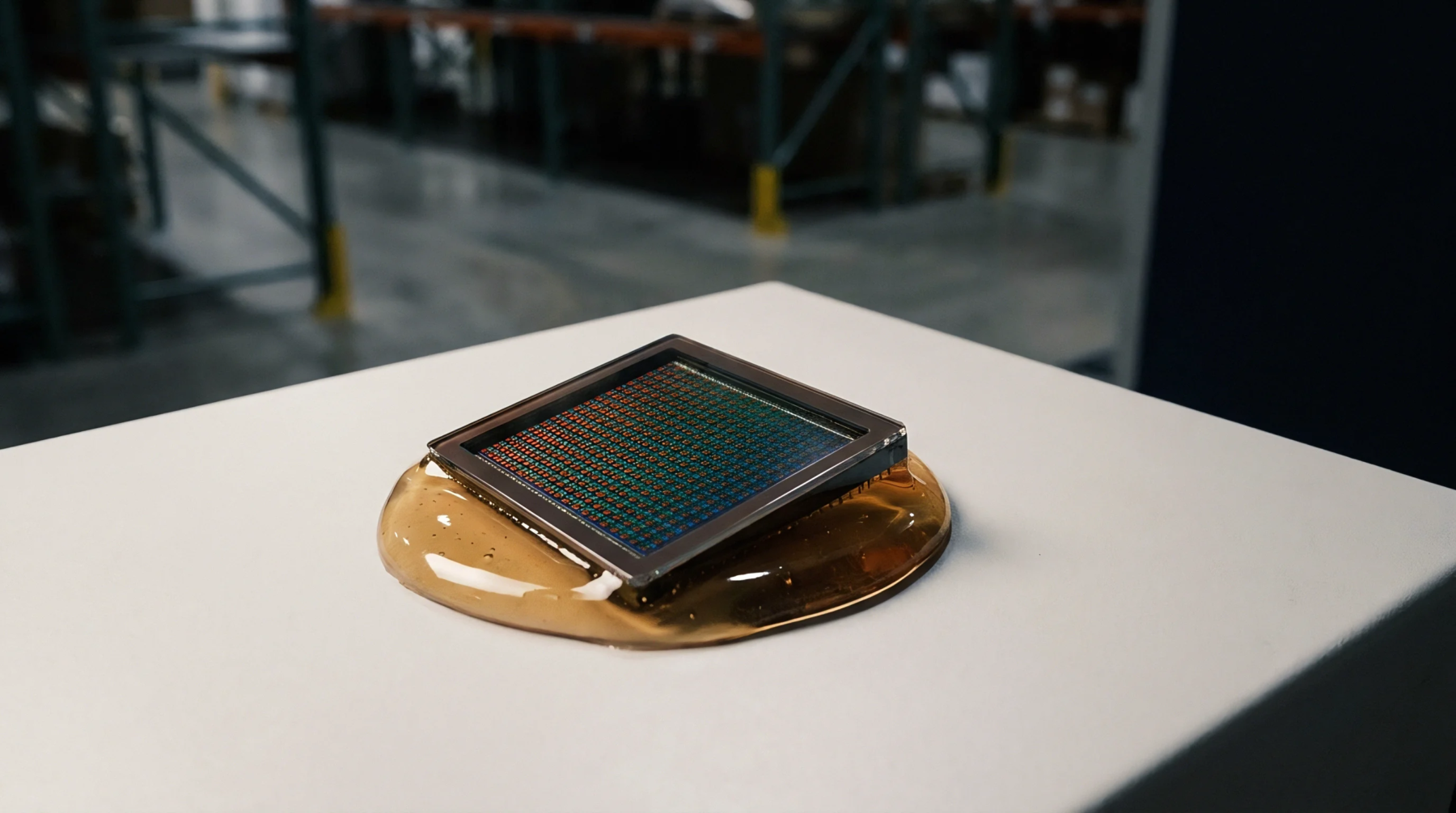
Microscopic electromechanical assemblies etched directly into crystalline semiconductor substrates convert physical dynamics into proportional electronic signals. In sensor production, silicon mems transducers provide compact sensing platforms for acceleration, angular rate, pressure and acoustic monitoring. The microfabrication workflow employs photolithography, deep reactive-ion etching and sacrificial layer release to craft suspended mechanical structures alongside integrated read-out circuitry.
The physical definition stops at the microscopic mechanical elements before conversion into digitized electrical output.
Thermal Stress
Mismatch between thermal expansion rates of the silicon die and mounting substrates introduces parasitic strain into sensing elements. Packaging stress degrades silicon mems zero-point bias stability and causes scale factor shifts over operating life. Die-attach materials must absorb mechanical strain without transferring shear forces to the micromachined proof masses.
Metrologists characterize this drift across thermal cycling chambers to construct digital compensation look-up tables stored in non-volatile sensor memory.
Transduction Principle
Capacitive readout architectures detect sub-angstrom movements of internal proof masses suspended by micromachined springs. As external forces displace these proof masses, interdigitated comb-finger structures experience capacitance variations that charge-amplifier stages convert into output voltages. Piezoresistive variants exploit stress-induced resistance changes across micro-machined diaphragms to capture high-pressure transients.
Both transduction modes rely on the high mechanical resilience and near-zero hysteresis of single-crystal silicon.
Packaging Isolation
Qualification standards require multi-axis shock testing up to ten thousand gravities to expose structural cleavage failures. Hermetic ceramic packages, metallic lids and vacuum cavity capping isolate internal resonators from atmospheric damping and moisture ingress. Environmental testing validates that hermetic seals prevent particulate contamination from locking micro-scale clearances between proof-mass combs.
The silicon mems architecture delivers repeatable mechanical transduction within compact physical envelopes.