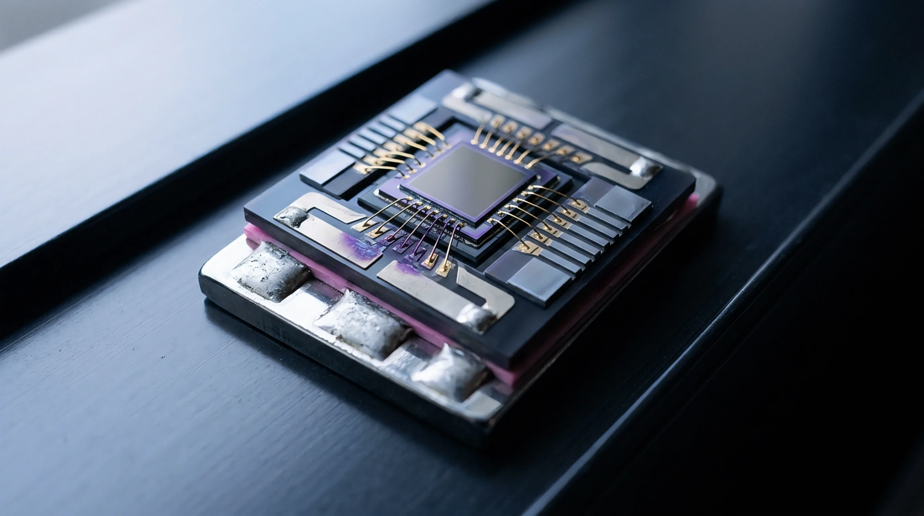
Micromachined Element
Monocrystalline silicon substrates etched with integrated resistor networks convert localized mechanical strain into proportional electrical resistance changes through the piezoresistive effect. The piezoresistive die operates as the primary electromechanical core in modern piezoresistive pressure transducers, force cells and structural strain sensors. Micromachining creates thin, compliant diaphragms or beams that flex predictably under applied mechanical pressure or force vectors.
This silicon element ceases to function predictably when temperatures exceed semiconductor junction limits or when applied stresses cause brittle silicon fracture.
Piezoresistive Transduction
Doped p-type or n-type regions diffused or ion-implanted into the silicon diaphragm form four interconnected resistors configured in a classic Wheatstone bridge layout. Applying mechanical pressure causes differential tensile and compressive stresses across the diaphragm surface, altering carrier mobility within the silicon crystal lattice. This mobility shift creates unbalance in the resistive bridge, producing an output voltage proportional to the applied excitation voltage and measured physical strain.
The crystal orientation of the silicon wafer dictates the magnitude and linearity of this elastoresistive response.
Instability Origins
Temperature variations cause substantial zero-signal offset drift and reduce bridge sensitivity due to the positive temperature coefficient of resistance and negative temperature coefficient of gauge factor. Package-induced mechanical stress transfers through die-attach adhesives, introducing parasitic offsets and hysteresis. Direct exposure to corrosive media degrades silicon surfaces or aluminum wire-bond pads, causing sensor drift or catastrophic open circuits.
High static line pressures can introduce subtle housing distortions that bias the output signal away from baseline calibration points.
Quality Qualification
Sourcing specifications define strict geometric, electrical and mechanical tolerances for incoming die lots before package assembly. Automated wafer-level probing measures baseline bridge resistance, isolation leakage currents and initial offset voltages across controlled thermal plates. Visual inspections under high magnification verify the absence of micro-cracks, metallization voids, contamination or diaphragm etching irregularities along perimeter edges.
Final lot acceptance requires statistical process capability verification to confirm that baseline sensitivities match procurement criteria.