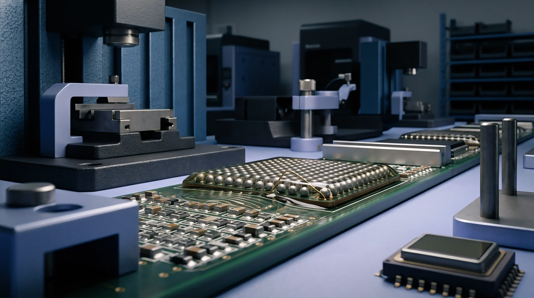
Component Encapsulation
Protective housing constructed from epoxy resin shields delicate semiconductor dies from moisture and physical damage. This type of molded package is created by placing the silicon chip on a leadframe and injecting a liquefied thermosetting polymer under high pressure. The polymer then solidifies to form a robust, chemically stable enclosure.
This physical boundary prevents external contaminants from reaching the wire bonds and the active silicon surface, which ensures long-term operational stability in harsh environments.
Thermal Characteristic
Heat dissipation across the resin body is a primary concern for high-power semiconductor devices. The material compound of a molded package is formulated with silica fillers to increase its thermal conductivity. If these filler concentrations are too low, the device may overheat and experience premature failure.
High temperatures can also cause the compound to degrade.
Stress Measurement
Internal mechanical stresses develop within the resin during the cooling phase of the encapsulation process. Technicians monitor molded package distortion by employing strain gauges or scanning acoustic microscopy. This measurement reveals internal delamination between the leadframe and the molding compound.
These voids can trap moisture and accelerate corrosion.
Reliability Standard
Accelerated stress testing defines the operational lifetime of packaged semiconductors. Standards for a molded package often require exposure to high humidity and elevated temperatures in specialized environmental chambers. The packaging must withstand these conditions without cracking or losing electrical isolation.
This verification is mandatory before commercial qualification.