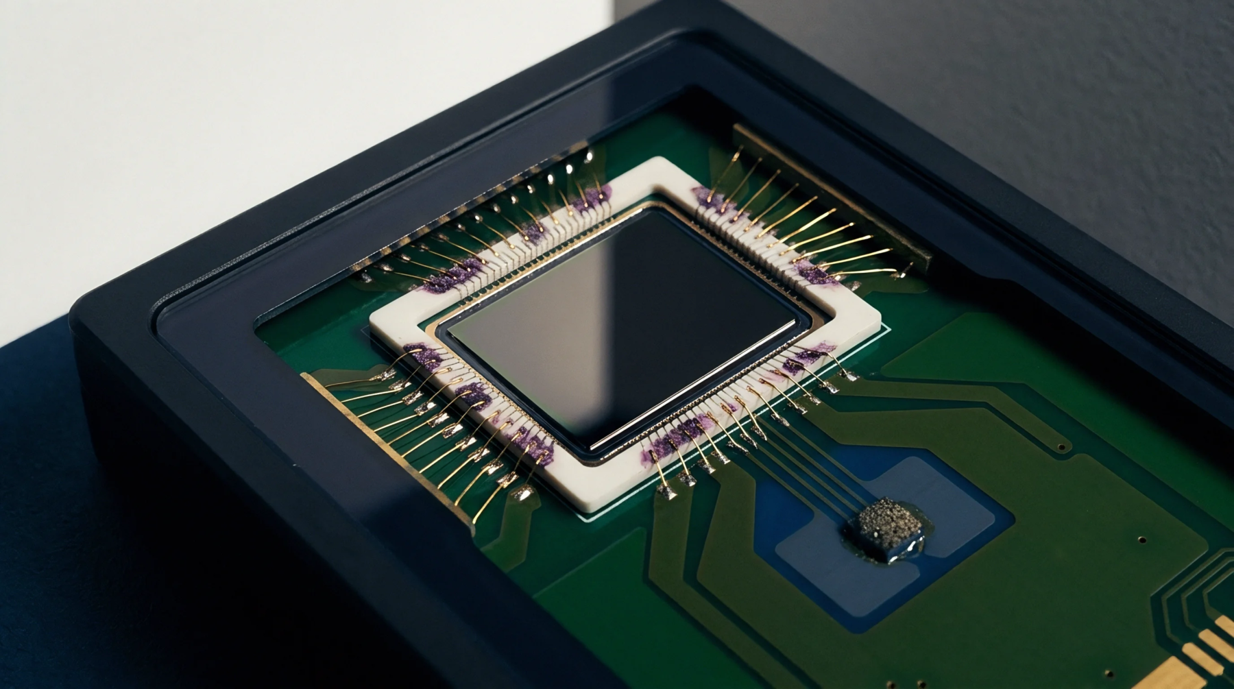
Mechanical Isolation
Semiconductor assembly technique that mechanically decouples a silicon chip from its carrier substrate to reduce internal tension. Utilizing floating die packaging prevents the transmission of mounting stress to sensitive sensing elements. This architecture uses a soft adhesive or a suspended bridge to hold the die in place.
The decoupling prevents external bending of the circuit board from altering the electrical properties of the silicon.
Stress Reduction
Protecting the chip from thermal expansion mismatch is the primary goal of this specialized construction. In floating die packaging, the sensing element is not rigidly bonded to the lead frame. This allows the package to expand and contract without pulling on the silicon structure.
Precision sensors such as gyroscopes and pressure gauges rely on this isolation to maintain their zero-point accuracy.
Packaging Architecture
Manufacturing these devices requires high-precision equipment to place the die on its flexible support. The floating die packaging design often incorporates a gel-filled cavity to provide additional damping against vibration. While this adds complexity to the production process, it significantly improves the stability of the device in high-vibration environments.
Engineers verify the integrity of the bond using acoustic microscopy and thermal imaging.
Measurement Integrity
Reliability of the sensor output is enhanced by eliminating the noise caused by package-induced stress. Because floating die packaging minimizes mechanical interference, the sensor can detect smaller changes in the measured environment. This performance is verified by testing the device under various mounting loads to ensure the offset does not shift.
High-end industrial sensors frequently utilize this method to achieve sub-percent accuracy.