Differential Resilience
Voltage isolation performance defines the maximum rate of change in input potential a galvanic barrier sustains before a logic state flips erroneously. Because common-mode transient immunity measures the delta voltage per unit of time across an isolation layer, it characterizes the stability of an optocoupler or digital isolator under high-speed switching noise. This parameter sits at the intersection of electromagnetic compatibility testing and high-voltage power electronics design.
Manufacturers verify these figures by applying high-slew-rate pulses to the isolation ground plane while monitoring the output signal for glitches or bit errors. A device meets a specification only when it maintains its designated logic state throughout the application of a specified dV/dt stress. High ratings indicate an ability to reject fast electrical events in environments containing inductive loads or motor drives.
Isolation Integrity
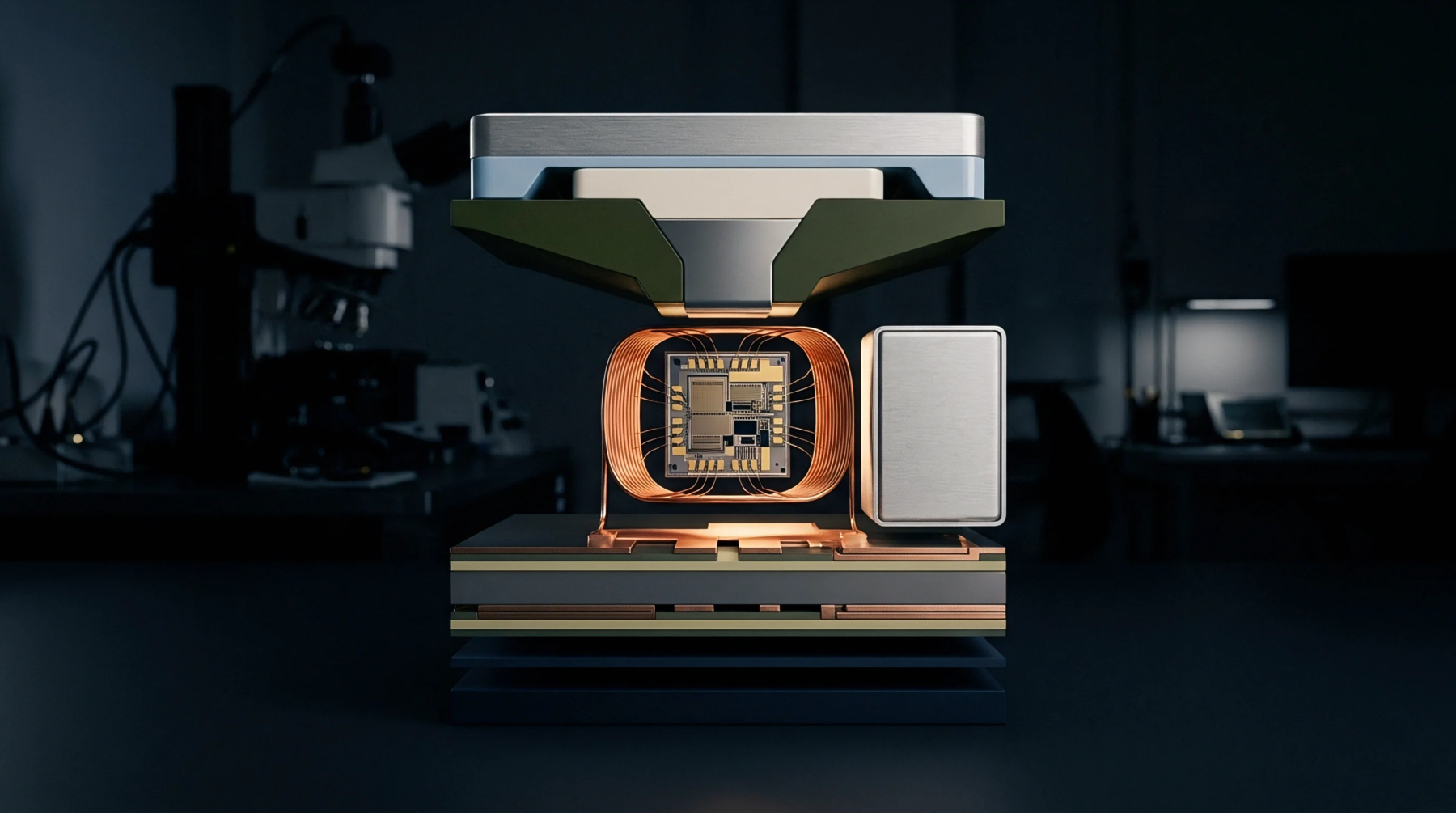
Capacitive or optical paths function as the primary mechanism for rejecting noise that hits both sides of a barrier simultaneously. A shift in the potential of one ground plane creates a displacement current flowing through the parasitic capacitance of the isolation boundary. If this current reaches a magnitude that triggers the internal receiver logic, a signal pulse appears at the output erroneously.
Designers calculate the threshold for this noise rejection by identifying the minimum gate charge required to switch the receiving transistor. Increasing the physical distance or dielectric strength between conducting plates reduces this parasitic coupling. Every component datasheet provides this limit as a kilovolt per microsecond value derived under controlled laboratory conditions.
Environmental Constraints
Installation in the field introduces variations that often erode the idealized specifications found in a laboratory datasheet. Large copper planes or long cable runs create secondary coupling loops that alter the effective noise path during operation. Layout engineers minimize these effects by placing decoupling capacitors near power supply pins to shunt transient currents away from sensitive logic gates.
Differential signalling techniques further improve performance by canceling out noise picked up equally on both lines. Proximity to high-power switching nodes remains the biggest factor affecting whether a component holds its rated immunity value during production cycles. Temperature extremes also shift the threshold voltage of internal semiconductors, which directly lowers the immunity limit as heat builds up within the package.
Verification procedures must account for these installation dynamics to ensure reliability in actual hardware applications.
Metrological Verification
Accuracy in measuring this property relies on generating clean pulses with rise times exceeding the expected immunity limit of the device under test. Specialized test fixtures deliver these fast waveforms while protecting the oscilloscope from damage caused by the high-voltage spikes. Calibration of these test setups requires careful grounding to prevent the measurement instrument from loading the signal being tested.
Errors in ground loop management during testing create false indications of failure when the device itself functions correctly. Precise characterization confirms the upper bound of the transient handling capability of a specific product design. Standardized test protocols establish the consistency required for commercial component interchangeability.