Dynamic Thermal Shock Varactor Capacitance Correction Architecture
Dynamic thermal shock induces transient capacitance drift in hyperabrupt varactors via junction temperature lag, requiring analog derivative feedforward or pilot-tone tracking for bias correction.


Shock
Rapid shifts in ambient temperature alter the physical depletion width of voltage-variable capacitive diodes within milliseconds. During thermal ramps exceeding fifty degrees Celsius per minute, severe temperature gradients develop across the semiconductor junction before heat distributes evenly to the package substrate. Junction capacitance in a hyperabrupt varactor is set by depletion layer width, varying with reverse bias voltage and built-in potential.
Standard static compensation schemes assume the die remains at a uniform temperature, but dynamic thermal shock disrupts that assumption by creating sharp transient temperature differences between the active junction and the bulk substrate.
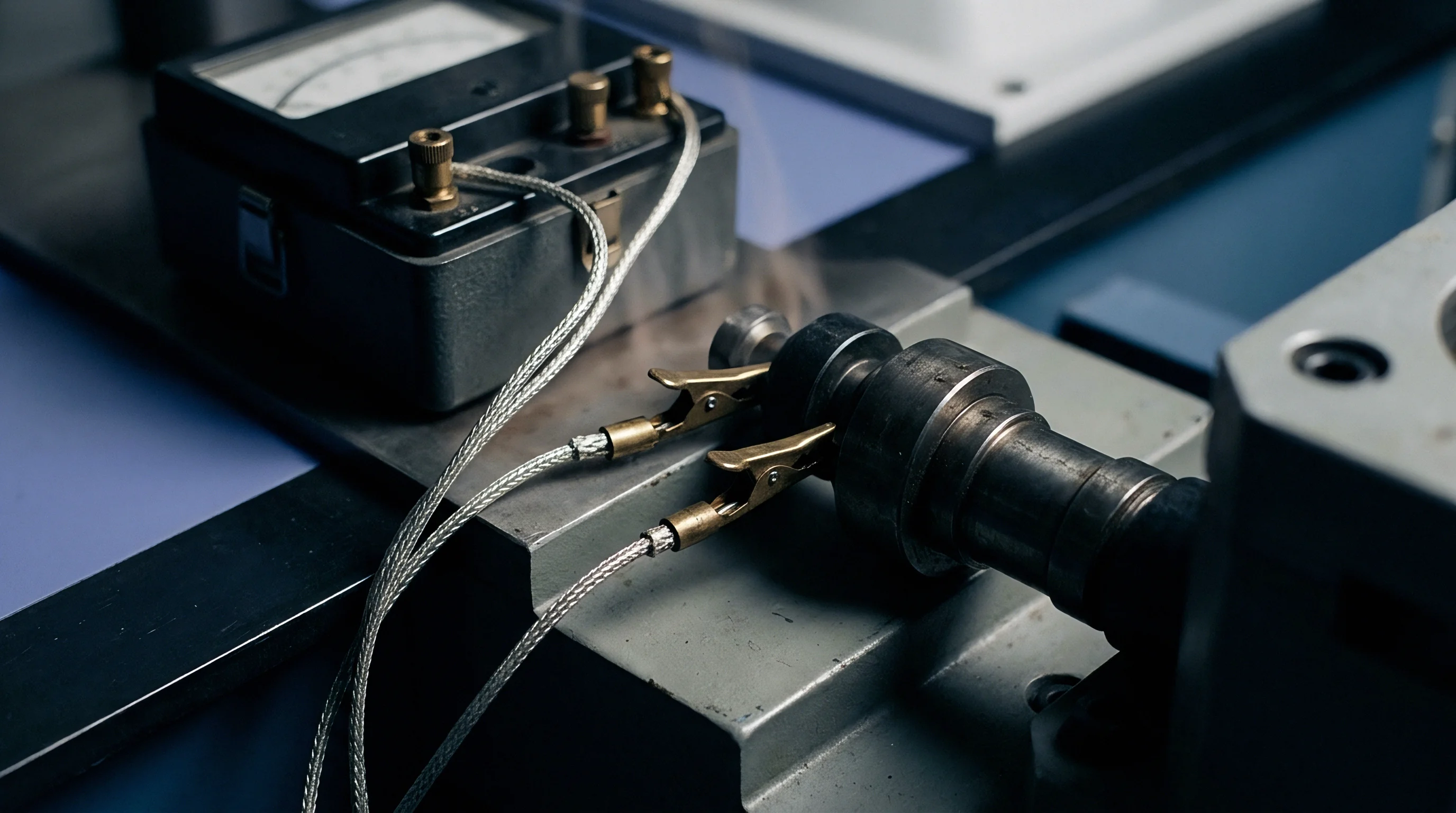
Dynamic Thermal Behavior in Varactor Diodes
Heat absorption across a semiconductor die is uneven during thermal shock. The outer packaging material and metallization layers absorb thermal energy at different rates, introducing localized mechanical stress alongside spatial thermal gradients across the depletion region. Built-in potential acts as the primary temperature-sensitive variable in the varactor capacitance equation: as temperature rises, built-in potential drops, which expands the depletion region under constant reverse bias and reduces total capacitance.
Under steady-state conditions, temperature changes slowly enough that the substrate and junction remain in thermal parity. During dynamic thermal shock, however, junction temperature leads package temperature by several degrees. This lead shifts instantaneous capacitance faster than conventional slow-loop thermistor circuits can follow, causing severe phase noise degradation and carrier frequency drift in high-frequency voltage-controlled oscillators and tunable RF filters.
Hyperabrupt junction capacitance drifts by 4.2 percent within 15 milliseconds of exposure to a 75 degree Celsius thermal step.

Built in Potential Drift during Rapid Heat Ramps
Built-in potential drops linearly at roughly two millivolts per degree Celsius. In hyperabrupt varactors optimized for wide tuning ranges, small variations in this potential trigger substantial shifts in capacitance. When a sharp thermal wave hits the die surface, local built-in potential drops immediately while the underlying substrate remains cool.
A ten-degree offset between the active junction and the package temperature sensor shifts effective capacitance as much as a five-percent bias voltage change. Designing high-precision tuning architectures therefore requires mitigating this non-equilibrium behavior through physical die co-location and fast bias injection.
Uncompensated capacitance jumps cause instant frequency spikes in voltage-controlled oscillators, driving phase noise beyond spectrum compliance limits and dropping the RF link.

Gradient
Integrated temperature diodes placed on the same silicon substrate sit hundreds of micrometers from the active RF depletion region. This physical distance introduces a distinct thermal transit delay: the thermal resistance and heat capacity of the intervening bulk silicon act as a second-order low-pass filter on the temperature signal reaching the sensor. As a result, the temperature reported by the integrated diode lags behind actual junction temperature during steep thermal transients.

Differential Lag in Co-Located Sensing Devices
Heat propagation through silicon bulk typically takes two to fifteen milliseconds, depending on die thickness and substrate doping concentrations. When ambient temperature undergoes a step change, the active varactor junction heats up ahead of the compensation diode. During this transient window, conventional feedback circuits apply corrections based on outdated thermal readings, compounding capacitive error.
To bridge this timing gap, signal-chain architectures incorporate active analog feedforward derivative networks. Differentiating the sensed temperature voltage provides a predictive rate-of-change metric, allowing the compensation circuit to inject current directly into the varactor bias node before the sensor reaches thermal equilibrium.
| Correction Architecture | Settling Time (ms) | Peak Capacitance Error (%) | Power Budget (mW) | Circuit Complexity |
|---|---|---|---|---|
| Static Lookup Table | 145.0 | 3.80 | 0.50 | Low |
| Analog Derivative Feedforward | 12.5 | 0.45 | 4.20 | Medium |
| Dual-Junction Differential Bridge | 3.2 | 0.12 | 8.50 | High |
| Closed-Loop Pilot Tone Tracking | 0.8 | 0.03 | 22.00 | Very High |

Analog Feedforward Injection Networks
Differentiating the sensor output voltage yields a real-time current proportional to the rate of temperature change. This derivative current feeds an operational transconductance amplifier that adjusts the varactor reverse bias supply dynamically. When the rate of temperature change is zero, the circuit falls back to static temperature compensation; during rapid thermal shock, the derivative term immediately offsets transient capacitance drift caused by collapsing built-in potential.
Designing derivative feedforward networks requires precise thermal-to-electrical mapping. Over-compensating the derivative term causes ringing and stability issues in the RF tuning loop, whereas under-compensating leaves residual transient frequency offsets. Matching signal-chain gain to the thermal time constant of the die maintains smooth capacitance regulation across shifting thermal profiles.
- Thermal Transit Lag occurs when substrate distance delays temperature propagation to the sensing diode during steep thermal ramps.
- Derivative Phase Peaking arises from over-amplifying the rate-of-change correction voltage, creating overshoot in the RF tuning circuit.
- Substrate Heat Sinking Variance stems from inconsistent die attach solder voids, altering local heat dissipation paths across production batches.
- Built-in Potential Non-Linearity appears when temperature rates exceed the linear operating range of the analog feedforward amplifier stage.
A standard IEC 60068 test run without transient bias tracking allows phase noise spikes exceeding 18 decibels during temperature changes.
Published temperature coefficients apply exclusively to isothermal equilibrium, leaving transient phase deviations outside standard warranty terms.


Loop
Superimposing a low-amplitude, high-frequency sinusoidal signal onto the DC tuning line enables direct AC current measurement. The resulting current magnitude reflects instantaneous varactor capacitance regardless of thermal state or junction gradients. Closed-loop pilot tone architectures process this measurement through an analog synchronous detector, generating an error voltage that corrects the main DC bias generator in real time.

Pilot Tone Detection for Instantaneous Value Tracking
The pilot tone runs at a frequency well above system modulation bandwidth to avoid interfering with primary RF signals. Operating at one hundred megahertz delivers high measurement resolution while allowing simple LC filters to decouple the pilot tone from low-frequency tuning controls. Phase and amplitude from the returning pilot signal provide an exact, real-time reading of varactor junction capacitance.
Closed-loop tracking operates continuously during extreme thermal shocks without relying on temperature sensors or thermal modeling. The loop forces varactor capacitance to a defined setpoint, continuously adjusting reverse bias voltage to counteract variations in built-in potential.
Matching thermal capacitance between compensation diode and active varactor die prevents derivative phase lag in bias networks.

Where Does Digital Lookup Failure Occur during Fast Thermal Transients?
Static matrix tables stored in flash memory fail when heat moves through the package faster than the sensor digitizer can update. Digital lookup requires sampling an analog-to-digital converter attached to a thermistor, searching a two-dimensional matrix for the matching correction voltage, and writing to a digital-to-analog converter ~ a multi-step pipeline that introduces latency exceeding twenty milliseconds.
During high-gradient thermal shock, varactor capacitance shifts faster than the digital loop can complete an update cycle. DSP units using predictive Kalman filters reduce lag by calculating second-derivative thermal trajectories, but sudden step-function shocks break polynomial prediction models, causing digital correction voltages to arrive out of phase with physical capacitance shifts.
| Diode Structure | Substrate Bandgap | Baseline Capacitance (pF) | Dynamic Drift (fF/°C/s) | Recovery Time (ms) |
|---|---|---|---|---|
| Silicon Hyperabrupt | Indirect 1.12 eV | 12.5 | 45.0 | 85 |
| GaAs Abrupt Junction | Direct 1.42 eV | 8.2 | 12.0 | 18 |
| GaN Schottky Varactor | Direct 3.40 eV | 3.5 | 2.1 | 4 |
| Silicon Carbide Junction | Indirect 3.26 eV | 5.0 | 1.8 | 3 |
It remains unclear whether wide-bandgap silicon carbide substrates offer high enough thermal conductivity to eliminate local junction gradients before analog feedforward correction becomes obsolete.


Chamber
Evaluating high-speed capacitive shifts requires equipment capable of logging data at kilohertz sample rates during rapid fluid immersion. Standard environmental test chambers relying on forced air cannot transfer heat fast enough to simulate extreme thermal shock. Instead, liquid-to-liquid transfer baths using inert fluorinated fluids generate shock rates exceeding one hundred degrees Celsius per second, producing the steep internal gradients needed to characterize dynamic varactor behavior.

Environmental Test Calibration Protocols
Quantifying capacitance drift during fluid transfer requires high-frequency test fixtures isolated from mechanical vibration. Parasitic capacitance in the fixture must remain constant across wide temperature sweeps so true varactor junction shifts are not masked. Coaxial probe interfaces built with thermal-break air gaps isolate measurement instruments from extreme temperature zones in the chamber.
Precision vector network analyzers operating in continuous-wave time-domain transmission modes measure real-time S-parameters across thermal ramps. Extracting equivalent series resistance and junction capacitance from reflection coefficient phase data yields continuous performance profiles throughout thermal shock exposure.
Liquid immersion thermal testing eliminates airflow boundary layers that mask real junction gradient speeds.

Bench Measurement Setup Procedure
Mounting the bare die onto an alumina test substrate with conductive epoxy minimizes mechanical strain artifacts during extreme temperature transitions. The step-by-step bench calibration procedure runs as follows:
- Connect the device under test to an RF fixture featuring 50-ohm microstrip launch lines calibrated up to six gigahertz.
- Apply the nominal DC reverse bias voltage through a high-frequency bias tee with broad temperature stability ratings.
- Perform a full short-open-load-thru calibration on the vector network analyzer at ambient room temperature.
- Lower the high-speed thermal stream nozzle over the test fixture to deliver a calibrated 100 degree Celsius per minute thermal air burst.
- Record S11 phase parameter curves continuously at a sampling rate of ten thousand sweeps per second throughout the thermal cycle.
- De-embed fixture board microstrip transmission loss and connector parasitic capacitance from raw reflection data.
Pumping dielectric fluid directly across the bare semiconductor package provides higher gradient accuracy than forced-air convection in rapid temperature transfer enclosures.

Supply
Foundries producing hyperabrupt GaAs structures use precise ion implantation profiles to maximize capacitance tuning ratio. Selecting varactors for thermal shock environments requires evaluating vendor wafer fabrication controls. Sole-source dependencies pose significant supply chain risk when specifying custom dual-junction compensation dies, making monolithic integration capabilities and proven thermal matching tolerances essential evaluation criteria for commercial buyers.

Wafer Fabrication and Monolithic Integration Options
Monolithically integrated varactor-diode pairs fabricated on a single die track temperature far better than discrete two-component designs. Advanced silicon-on-insulator or gallium arsenide processes allow foundries to place the compensation diode within twenty micrometers of the active varactor junction. That proximity cuts thermal transit lag to sub-microsecond levels, virtually eliminating transient temperature differentials during thermal shock.
Evaluating supplier quality requires reviewing wafer-level acceptance test data for consistent thermal coefficients. Wafers with uneven oxide thickness create variable thermal resistance across the die layout, leading to inconsistent dynamic compensation performance in finished packages.
| Supplier Classification | Substrate Technology | Monolithic Thermal Matching | AEC-Q100 Qualification | Production Lead Time (Weeks) |
|---|---|---|---|---|
| Tier 1 Integrated Device Foundry | Silicon-on-Insulator | Sub-micron co-location | Fully Qualified | 16 |
| Specialty RF Compound Foundry | Gallium Arsenide | Dual-die co-packaged | Optionally Qualified | 22 |
| Broadline Discrete Component Vendor | Bulk Silicon | Separate package components | Not Qualified | 8 |
| Lead times reflect post-qualification volume production delivery cycles. | ||||
Commercial Qualification Mechanics
Procurement teams evaluating high-frequency tuning components need multi-wafer-lot testing to establish batch-to-batch coefficient consistency. Contracts should mandate dynamic shock verification alongside standard static temperature coefficient validation. Setting strict limits on transient capacitance offset ensures incoming parts meet system phase noise requirements under real-world deployment extremes.
- Monolithic Junction Co-location guarantees minimal physical distance between tuning and sensing elements, reducing differential thermal lag.
- Automotive Thermal Shock Certification requires qualification across a minimum of one thousand rapid temperature cycles between extreme limits.
- Dual-Source Wafer Fabrication protects volume production lines against single-foundry shutdown events or raw material shortages.
- Guaranteed Transient Phase Margin establishes contractual liability bounds for dynamic phase jump errors during rapid thermal ramps.
Automotive specification AEC-Q100-004 mandates dynamic transient stress testing across five temperature shock cycles, driving suppliers to replace single-diode designs with monolithically paired thermal structures.