Testing Interface
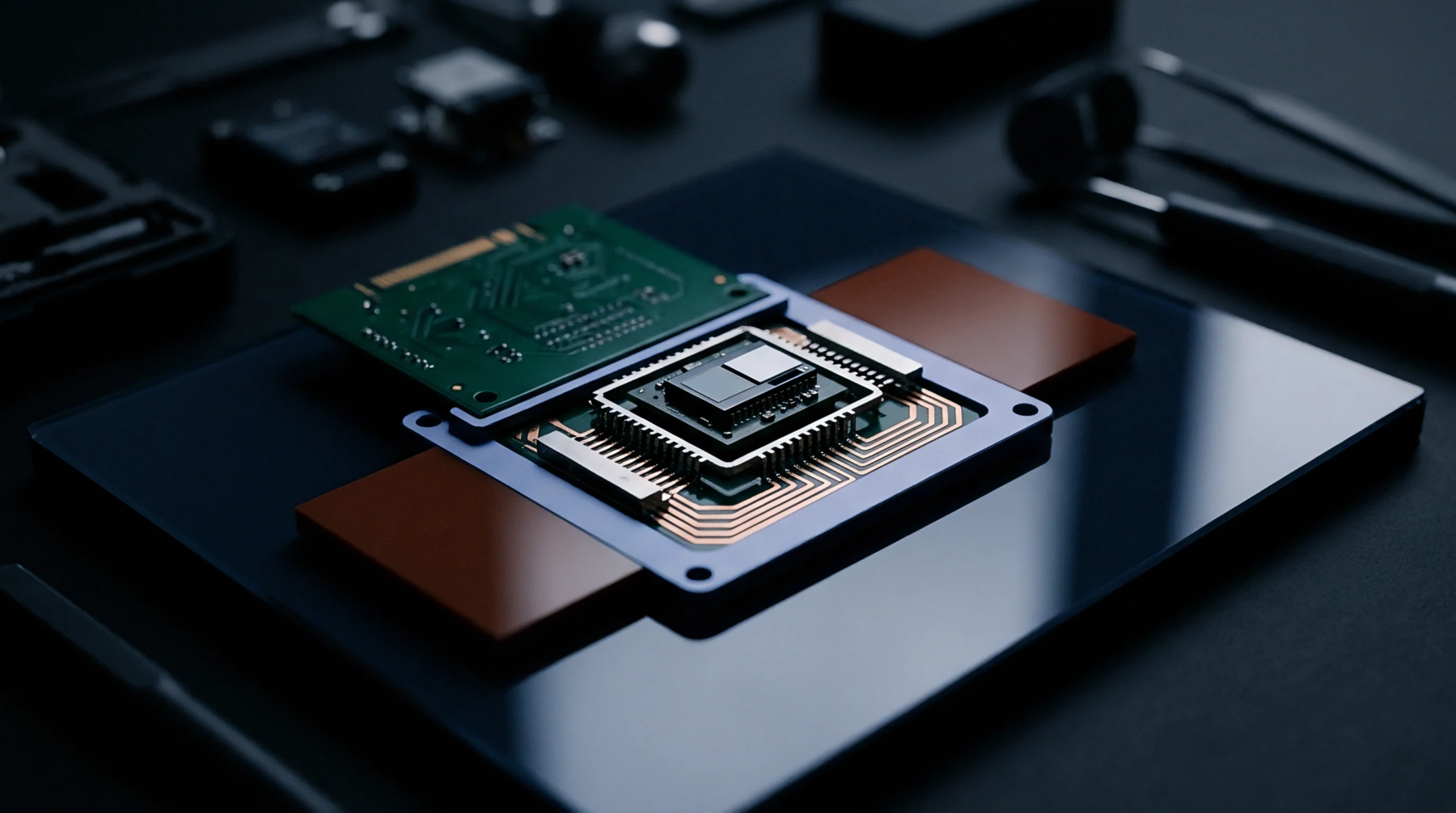
Electrical signals retrieved from individual die on a semiconductor wafer provide essential data on the performance and yield of the manufacturing process. The wafer probe readout occurs during the functional testing phase before the wafer is diced into separate chips. It utilizes a probe card with fine needles or bumps that make temporary contact with the bond pads of the circuit.
Signal Integrity
High-frequency measurements require management of the impedance and parasitic capacitance of the probe interface. As the wafer probe readout progresses, the contact resistance between the probe tip and the pad must remain stable to ensure accurate voltage and current readings. Cleaning the probe tips periodically removes debris and oxide buildup that could interfere with the signal.
Metrology Data
Results from the test are compiled into a wafer map that shows the geographic distribution of passing and failing units. This wafer probe readout identifies systematic defects related to specific process steps, such as lithography variations or etching non-uniformity. Analyzing this map helps engineers optimize the production parameters to increase the overall yield.
Throughput Consideration
Modern testing stations use parallel probing to measure multiple die simultaneously, which reduces the total time required for the wafer probe readout.