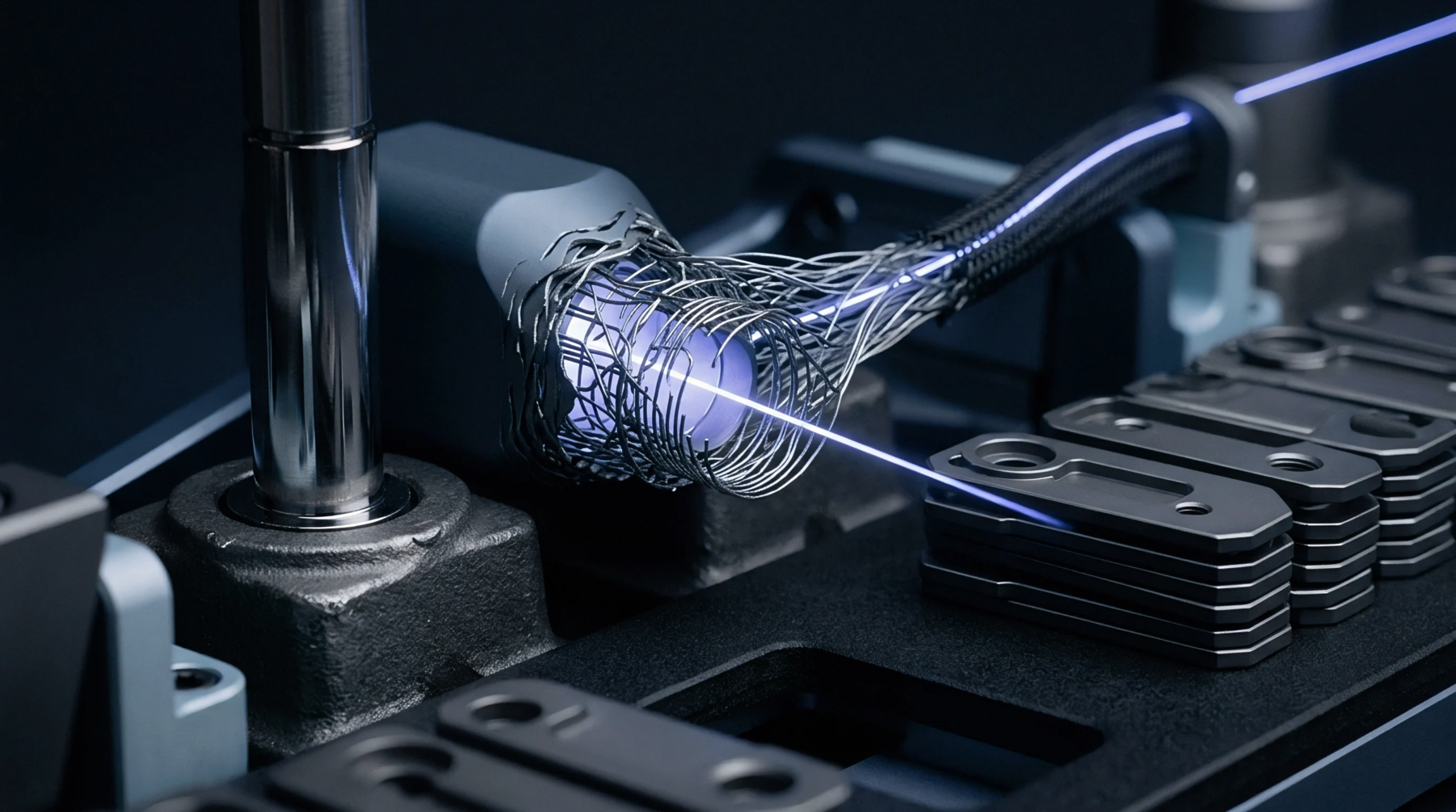
Thermodynamic Micro-Strain Relaxation in Die Attach Adhesives during Thermal Soak
Thermal soak accelerates die attach viscoelastic micro-strain relaxation, reducing shear stress while driving physical aging, interface delamination, and Rth growth.
Metrological practice defines thermal resistance growth as the progressive accumulation of parasitic temperature drops across internal package interfaces during active operational deployment. Semiconductor devices experience degradation at die attach layers because mechanical stress and thermal cycling drive microscopic void propagation over operational years. Absolute junction temperature measurement requires specialized calibration benches where transient dual temperature testing isolates interfacial impedance shifts from ambient variations.
Reference standards dictate that primary verification occurs under strict constant power conditions to prevent self heating artifacts from skewing baseline voltage drop readings. Manufacturers establish static acceptance thresholds during initial production burn in runs to screen out assemblies prone to rapid interfacial delamination under field loads.
Intermetallic compound formation accelerates whenever sustained high current densities traverse dissimilar metallurgical boundaries inside power electronics packages. Microscopic voids multiply across these bonding planes because atomic diffusion rates differ significantly between copper leadframes and gold wire bonds operating at elevated temperatures. Calibration laboratories quantify this physical deterioration by tracking forward voltage parameters on integrated p-n junctions during controlled power cycling sequences.
Subsequent data processing converts electrical measurements into accurate thermal impedance values by applying known transient thermal response functions. Field instruments measure junction temperature rise relative to case temperature references to calculate real time interfacial health indexes for active power modules.
Mechanical compliance mismatches between encapsulant resins and underlying silicon dies generate permanent shear strains throughout extended thermal excursions. Temperature fluctuations force continuous expansion and contraction cycles that gradually fracture solder joints supporting high power semiconductor substrates. Automated test equipment detects these structural failures by monitoring subtle increases in transient cooling curves immediately following power shutdown events.
Production facilities rely on accelerated life testing chambers to simulate decades of field exposure within compressed operational windows. Metrologists apply mathematical deconvolution algorithms to raw cooling curves in order to separate die attach degradation phenomena from external heatsink mounting anomalies.
Standardized acceptance criteria dictate that any package exhibiting an interfacial impedance increase exceeding specific percentage boundaries fails reliability qualification protocols. Quality assurance engineers verify these degradation limits by comparing post stress calibration curves against pristine baseline scans recorded prior to environmental testing. Environmental test chambers maintain precise ambient control to ensure that external thermal fluctuations do not compromise the accuracy of subtle junction voltage measurements.
Final compliance verification certifies that semiconductor assemblies retain adequate heat dissipation capacity throughout their intended operational lifecycle. Systematic interfacial monitoring prevents catastrophic field failures by identifying microscopic structural degradation before devices exceed critical thermal thresholds.
Thermal soak accelerates die attach viscoelastic micro-strain relaxation, reducing shear stress while driving physical aging, interface delamination, and Rth growth.
Expertise is a utility, not a secret. sentiention™ publishes its working knowledge as open reference: intelligence layer covering the materials it sources, the markets it enters, and the reference that serves both.