Process Sequence
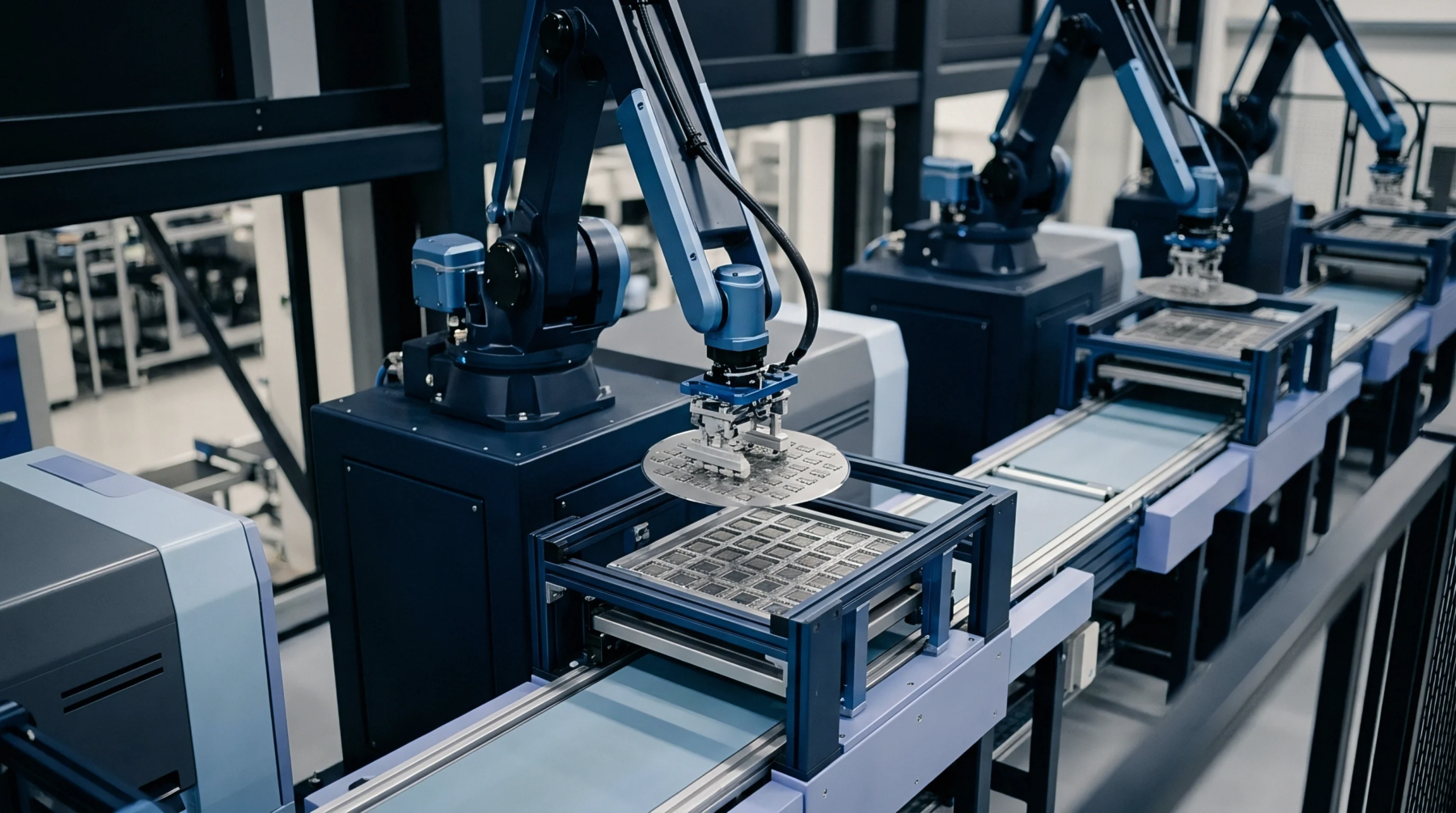
Sequence of cleanroom processes used to etch and shape three-dimensional structures into semiconductor substrates for pressure detection. Advanced mems pressure sensor microfabrication involves photolithography, thin-film deposition, chemical etching and bulk micromachining to create a flexible diaphragm. This structure deforms under external pressure to produce a measurable electrical change.
Consistency in the etch rate determines the final thickness of the sensing element, which dictates the pressure range and burst strength of the sensor.
Dimensional Control
Deep reactive ion etching allows for high aspect ratio structures with vertical sidewalls. In mems pressure sensor microfabrication, the precision of the diaphragm thickness directly influences the sensitivity of the finished device. Variations of only a few nanometres can shift the full-scale range by several percent.
Wafer Bonding
Hermetic sealing of the reference cavity occurs during the final stages of production. Anodic bonding joins the structured wafer to a glass base. This mems pressure sensor microfabrication step creates the stable vacuum reference required for absolute pressure measurement.
Metrological Qualification
Final inspection uses scanning electron microscopy and white light interferometry to verify the geometry, thickness, alignment and stress. Any mems pressure sensor microfabrication run is qualified by testing a subset of the wafer for burst pressure and linearity. These tests ensure the mechanical properties meet the design specifications before the wafer is diced into individual chips.