Layout Balance
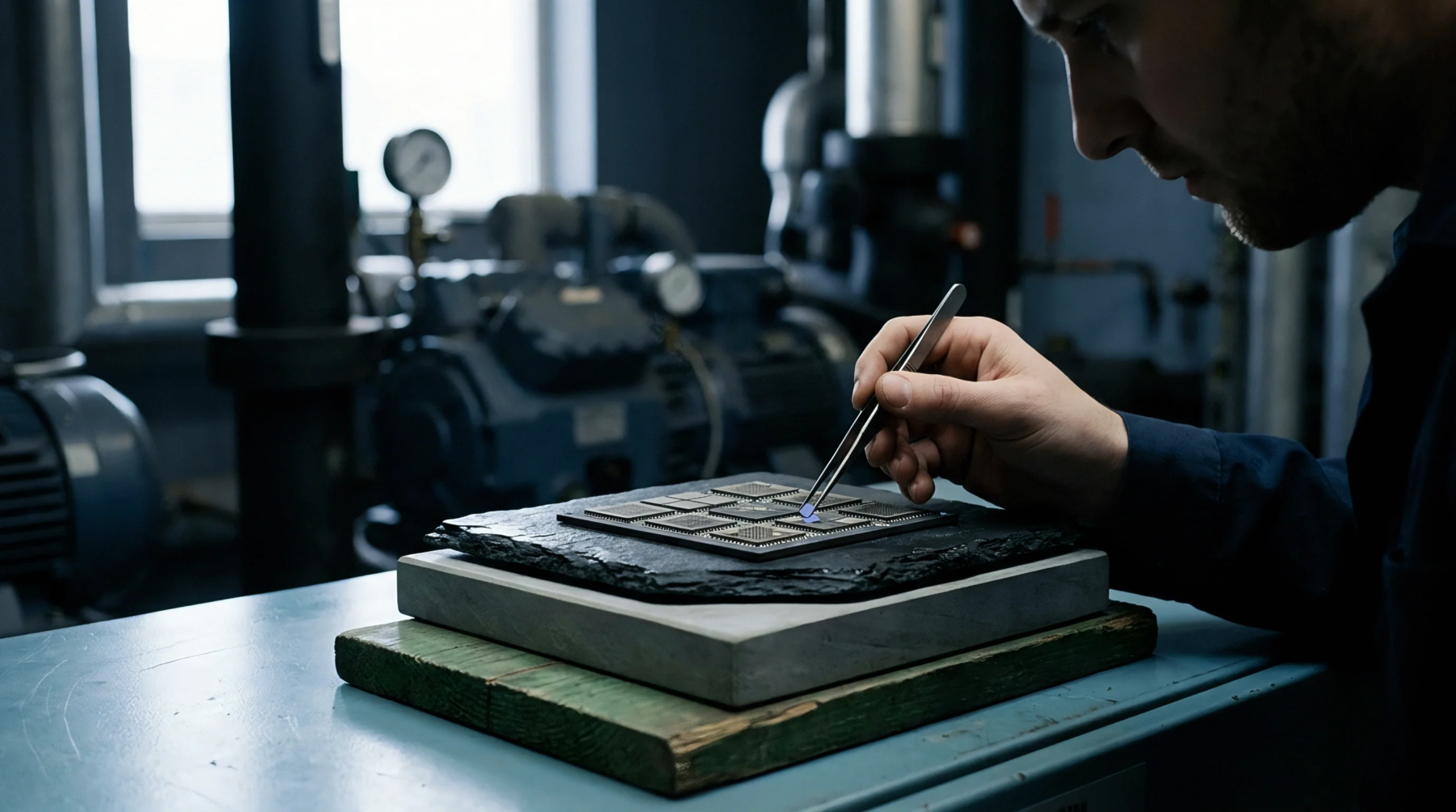
Geometric uniformity across printed circuit board surface-mount footprint pads guarantees balanced surface tension forces during solder reflow processing. Designing circuit boards with strict land pattern symmetry prevents mechanical rotational moments from pulling leadless integrated circuit packages out of alignment. Identical copper land geometries expose matching volumes of solder paste to uniform thermal profiles across opposite package edges.
Traces exiting pads balance heat dissipation to stop uneven paste melt times from causing tombstoning or partial lifting. The geometric scope of pattern balance governs copper pad sizing, solder mask relief dimensions, thermal relief connections and adjacent trace entry routing.
Reflow Mechanics
Molten solder dynamics exert self-centering capillary forces that align component terminations onto matching substrate copper lands. Maintaining land pattern symmetry allows liquid surface tension to pull the sensor body into true center without skew. Unequal land geometries disrupt fluid force vectors, pivoting miniature leadless packages toward the pad with greater solder volume.
Asymmetrical heat sinking delays wetting on grounded pins, generating phase discrepancies in alloy melting. Solder bridging risks elevate when shifted packages contact adjacent routing tracks.
Thermal Dissipation
Unequal thermal conduction pathways between opposing printed circuit board pads induce uneven alloy liquidus timing across high-density leadframes. Proper land pattern symmetry incorporates matched copper neck-down widths and identical thermal relief spoke counts on ground-connected lands. Direct trace connections into large ground planes withdraw heat much faster than traces entering isolated signal paths.
Solder pastes on cooler pads melt later, generating wetting delays that twist quad flat no-lead packages. Component displacement during liquidus phases increases internal shear stress on cooling solder joints.
Stress Distribution
Operating temperature excursions generate cyclical thermomechanical strain across surface-mount solder interconnects due to coefficient of thermal expansion differences between the component package and the circuit board. Symmetrical land patterns distribute this cyclic shear strain evenly across all peripheral joints, eliminating localized stress concentrations that trigger premature solder fatigue. Irregular footprints concentrate thermomechanical fatigue on undersized pads, accelerating micro-crack growth through joint interfaces.
Automated optical inspection systems identify board warpage and pad asymmetry by scanning component rotation angles against reference layout footprints. Mechanical reliability testing verifies shear survival margins under repeated thermal shock exposure. Symmetrical solder geometries guarantee uniform stress relaxation paths across peripheral package terminations.