Geometric Deviation
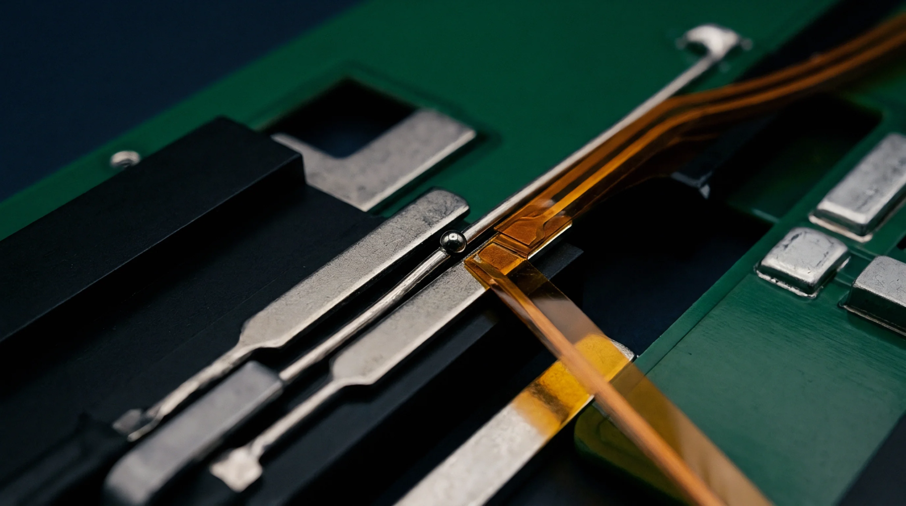
Planar deviation of a printed circuit board under thermal or mechanical loading represents a geometrical distortion that impedes automated solder paste printing and component placement. This physical anomaly, known as board warp, is measured as the maximum displacement from a reference flat surface divided by the diagonal length of the board. The IPC-A-600 standard governs the permissible limits for this distortion.
Thermal Cause
Thermal expansion mismatch between the copper cladding and the glass-epoxy substrate during laminating or soldering initiates the internal stress that deforms the substrate. This imbalance is particularly pronounced in asymmetrical layer stackups. Symmetric design prevents the asymmetrical stress distribution that causes board warp during cooling cycles.
Measurement Method
Optical profiling scans the surface against a reference plane to quantify the deviation. This scanning yields a grid of displacement points.
Tolerance Limit
Permissible thresholds typically depend on the presence of surface-mount components, where a limit of zero point seven five percent of the diagonal dimension applies to most boards. For boards utilizing fine-pitch ball grid arrays, the limit drops to zero point five zero percent to prevent solder bridging and open joints. Production facilities verify this threshold after both lamination and solder-mask curing.