Asynchronous Peripheral Clock Stretching in Surface Mount Sensor Packages
Asynchronous SCL stretching requires host firmware timeouts above 35 ms and land patterns designed to isolate internal RC relaxation oscillators from reflow strain.


Hold
Digital surface mount sensor packages running I2C or SMBus interfaces frequently assert low signal states on the clock line during internal measurement cycles. This state assertion halts host communication by holding the Serial Clock (SCL) line near system ground, preventing the master transceiver from driving subsequent clock pulses until internal analog front ends complete their conversion routine.

Electrical Mechanics of Bus Clock Stretching
When an integrated sensor circuit completes an analog conversion, the internal state machine overrides the external Serial Clock line. The peripheral ASIC sink transistor pulls SCL below the logic low threshold, typically specified at 0.3 times the supply voltage. The host microcontroller senses SCL suppressed below the logic high threshold of 0.7 times supply voltage and suspends clock signal generation.
Asynchronous peripheral clock stretching occurs because internal conversion timing relies on on-chip RC relaxation oscillators rather than the host bus clock. SCL low durations range from 10 microseconds in high-speed optical packages to 28 milliseconds in multi-channel environmental units.
Interface timing constraints vary dramatically between package implementations. Small LGA and DFN forms host compact silicon dies where internal state machines process sensor data in tight hardware pipelines. Larger ceramic or gel-filled packages often incorporate digital signal processing engines that execute FIR filtering and polynomial temperature compensation onboard, driving long SCL low extensions.
| Package Type | Typical Die Area (mm²) | Interface Protocol | Max Stretch Duration (ms) | Stretch Trigger Event |
|---|---|---|---|---|
| LGA-8 (2.0 x 2.0 x 0.9 mm) | 1.21 | I2C Fast-Mode | 0.85 | ADC Sample Integration |
| DFN-6 (3.0 x 3.0 x 0.75 mm) | 2.25 | I2C Fast-Mode Plus | 4.20 | DSP Compensation Filter |
| QFN-16 (4.0 x 4.0 x 0.85 mm) | 4.84 | SMBus 3.0 | 25.00 | EEPROM Non-Volatile Write |
| WLCSP-12 (1.5 x 2.0 x 0.5 mm) | 0.75 | I2C Standard-Mode | 12.50 | Core Thermal Stabilization |

Internal Oscillator Latency in Sensor ASIC Packaging
On-chip RC relaxation oscillators generate the timing pulses required to drive internal analog front ends. These integrated clock sources exhibit temperature coefficients up to 250 parts per million per degree Celsius. Silicon strain and supply voltage fluctuations alter the baseline relaxation frequency, shifting the duration of SCL low states during operation.
Internal clocks drift under thermal stress. When an internal clock slows, peripheral conversion delays extend, holding the physical SCL line low longer than specified in nominal room-temperature datasheets.
The component vendor attributes extended low clock pulses to dynamic execution adjustments within internal DSP filtering stages under elevated ambient noise conditions.
Host controllers that fail to monitor SCL high-to-low transitions risk corrupting multi-byte read frames. When a host assumes fixed conversion windows without polling physical line states, data bits read from SDA return corrupted byte sequences. Firmware architectures demand explicit hardware state verification before each clock edge generation.
Reflow
Surface mount mounting processes introduce significant thermo-mechanical stress into sensor packages during thermal assembly. Lead-free reflow profiles peaking at 260 degrees Celsius subject organic substrates, epoxy mold compounds, and silicon dies to differential thermal expansion.
Thermomechanical Stress and Internal Clock Drift
Thermal expansion mismatches between organic printed circuit board substrates and silicon dies deform internal microstructures. Standard FR-4 substrates expand at 14 to 17 parts per million per degree Celsius along the planar axis, while silicon expands at 2.6 parts per million per degree Celsius. Solder joint solidification anchors package pads to board land patterns under peak thermal strain.
Post-cooling epoxy mold shrinkage generates baseline compressive stress ranging from 300 to 600 microstrain across the integrated circuit area.
Piezoresistive effects in silicon alter the electrical resistance of integrated polysilicon and diffusion resistors inside RC clock networks. A shift in resistance changes the charging time constant of internal relaxation nodes, widening peripheral clock stretch durations across production batches. Silicon strain modifies internal oscillator frequencies.
- Board heating during peak thermal immersion expands the substrate matrix at 15 ppm per degree Celsius.
- Solder joint solidification anchors package pads to board land patterns under maximum thermal strain.
- Post-cooling epoxy mold shrinkage generates differential compressive forces across the integrated die area.
- Piezoresistive impedance shifts alter internal bias currents within the relaxation oscillator array.
- Oscillator period variance extends peripheral processing cycles beyond nominal factory datasheet window limits.
A post-assembly package strain of 450 microstrain shifts internal RC clock frequency by 8.2 percent at room temperature.

Substrate Warpage and Package Moisture Sensitivity
Package dimensions dictate how environmental humidity absorption alters internal mechanical package tension. Epoxy mold compounds absorb moisture over time, expanding hygroscopically according to their moisture sensitivity level classification under JEDEC J-STD-020 standards.
Moisture absorption expands package mold compounds. During reflow assembly, trapped water turns to high-pressure steam, creating micro-delaminations between the leadframe die pad and the encapsulation resin. Mold delamination reduces mechanical clamping force on the silicon die, shifting oscillator baseline frequencies and altering clock stretch timing parameters over the product lifecycle.
Ignoring package thermomechanics produces intermittent bus timeouts on two percent of assembled boards after environmental stress testing.
Bus
Open-drain physical interconnect lines rely entirely on external pull-up resistors to return SCL to logic high levels. When an internal sensor peripheral releases its clock stretching hold state, line capacitance governs the voltage rise trajectory from logic low back to VDD.
Physical Signal Integrity under SCL Pull-Up Dynamics
Total line capacitance dictates the minimum pull-up current needed to achieve compliant edge rise times. SCL line capacitance comprises printed circuit board trace routing parasitics, host pin capacitance, and peripheral input capacitance. Per I2C bus specifications, maximum allowable rise time for Fast-Mode operation stands at 300 nanoseconds, while Standard-Mode allows up to 1000 nanoseconds.
Calculating the maximum allowable pull-up resistance uses the standard bus RC timing relationship. Open-drain buses require pull-up resistors. Rise times degrade with parasitic capacitance.
High pull-up resistance causes slow edges.
Calculating pull-up resistor sizing against total bus capacitance follows standard open-drain timing equations:
R_p(max) = t_r / (0.8473 C_b)
Assuming a total bus capacitance of 150 picofarads and a target Fast-Mode rise time of 300 nanoseconds, maximum pull-up resistance calculates to 2.35 kilohms. Minimum pull-up resistance depends on the current sinking capability of the weakest peripheral driver on the bus, specified at 3 milliamperes for a standard 0.4 volt output low level, yielding a minimum resistance of 967 ohms at 3.3 volt VDD.
Designing pull-up networks for maximum speed without measuring total line capacitance guarantees intermittent clock stretching timeouts.
Multi-Slave Contention and High-Speed Mode Latency
Placing multiple peripheral devices on a shared two-wire line creates complex interaction windows during stretch phases. If peripheral device A completes conversion and releases SCL while peripheral device B continues stretching, the physical line remains suppressed at logic low. Host controllers must refrain from initiating clock pulses until every active peripheral releases the open-drain SCL net.
- Mid-Level Voltage Plateaus occur when a stretching device releases SCL while an adjacent slave holds the line low during address matching.
- Spurious Start Conditions arise if host clock generators re-assert SCL high before SDA transitions complete during extended stretch intervals.
- Clock Low Timeout Triggers activate prematurely when peripheral processing duration exceeds fixed hardware timer limits.
- Bus Deadlocks lock the physical interface permanently if the peripheral fails to release SCL following an internal execution stall.
| Protocol Standard | Max Bus Speed (kHz) | Max SCL Rise Time (ns) | Allowed Stretch Time | Timeout Support |
|---|---|---|---|---|
| I2C Standard-Mode | 100 | 1000 | Uncapped | Optional |
| I2C Fast-Mode | 400 | 300 | Uncapped | Optional |
| I2C Fast-Mode Plus | 1000 | 120 | Uncapped | Optional |
| SMBus 3.0 | 1000 | 120 | 25 ms to 35 ms | Mandatory |
| Methods Note: Data extracted from NXP UM10204 and System Management Bus Specification Version 3.0. SMBus imposes hard timeout bounds on SCL low assertions to prevent system bus hangs. | ||||
Matching pull-up impedance to actual trace capacitance prevents false clock edge detection during peripheral release steps.

Driver
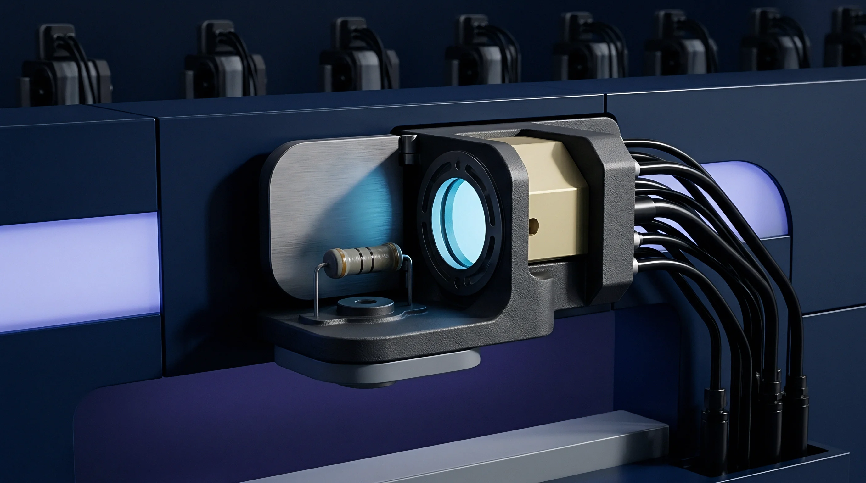
Host firmware architecture determines whether asynchronous clock delays cause system execution stalls or pass transparently through the software stack. Hardware I2C peripherals inside mainstream microcontrollers exhibit varying levels of silicon maturity regarding physical clock stretching support.
How Does Host Timeout Logic Fail during Stretching?
Hardware I2C controllers in mainstream microcontrollers frequently implement clock stretching detection through dedicated hardware timers. When a sensor peripheral pulls SCL low beyond expected bit time windows, internal hardware state machines lock up if the peripheral peripheral controller lacks asynchronous clock synchronization logic. Hardware state machines lock up frequently.
Certain microcontroller silicon revisions freeze peripheral interrupt flags when SCL stays depressed during a register read sequence. Software drivers built around simple polling loops freeze indefinitely, stalling execution threads in real-time operating systems unless bounded by software watchdog routines.
Compliance with SMBus 3.0 Section 3.1.3 limits SCL low duration to 35 milliseconds, forcing hardware bus resets when exceeded.

State Machine Recovery and Bus Clear Sequences
Handling stuck signal states demands explicit recovery routines written directly into the communications layer. When a peripheral device hangs mid-transaction with SCL or SDA held low, host software must bypass the dedicated hardware peripheral, reconfigure interface pins as general-purpose outputs, and manually clear the line.
- Hardware Timer Allocation assigns an independent hardware counter to monitor SCL low durations on every transaction.
- GPIO Mode Fallback enables software bit-banging re-initialization whenever hardware peripheral state machines freeze.
- Non-Blocking IO Wrappers execute peripheral reads inside asynchronous tasks to prevent real-time operating system scheduler starvation.
- Bus Recovery Routines toggle SCL nine times manually to clear unreleased slave open-drain drivers.
Nine clock pulses clear stuck buses. Re-asserting a STOP condition following nine SCL toggles restores communication with hung peripheral state machines without cycling power to the surface mount package.
Standard procurement documentation specifies that peripheral drivers failing to execute nine-clock recovery sequences upon timeout detection forfeit compliance certification under automated hardware test frameworks.

Audit
Verification of peripheral clock stretching behavior requires automated oscilloscope captures under combined thermal and voltage stress conditions. Standard functional test benches operating at room temperature miss transient clock extensions that occur only at supply voltage and temperature extremes.
Logic Analyzer Capture of Asynchronous Pulse Stretching
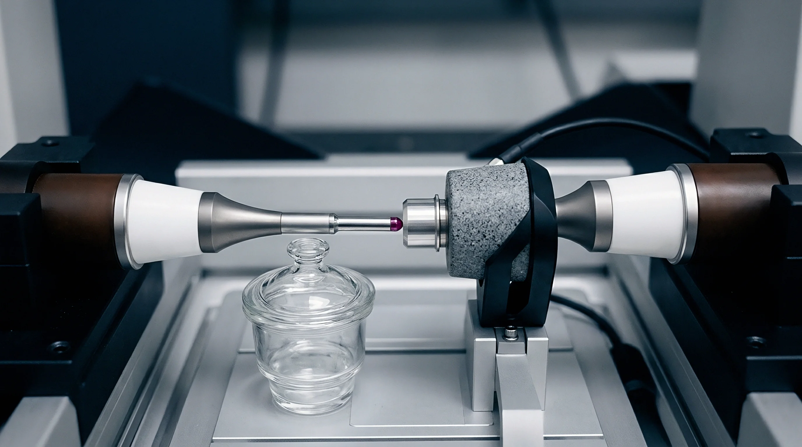
High-sample-rate protocol monitors detect transient stretch extensions that pass unobserved during routine bench evaluation. Testing requires calibrated scope triggers. Logic analyzers set to capture SCL low pulse widths exceeding nominal clock half-periods record exact peripheral execution windows across millions of transaction cycles.
| Test Parameter | Sampling Rate | Trigger Condition | Pass Criteria |
|---|---|---|---|
| SCL Low Duration | 100 MS/s Minimum | SCL Low > 1.25 x Period | Pulse Duration < 25.0 ms |
| SCL Edge Transition | 1 GS/s Minimum | Edge Rise Time Measurement | Rise Time < 300 ns (Fast-Mode) |
| VOL Noise Margin | 500 MS/s Minimum | VIL Threshold Trapping | VOL Voltage < 0.4 V at 3 mA |
| Recovery Latency | 100 MS/s Minimum | SCL Release to SDA Valid | Data Valid Setup > 100 ns |

Corner-Lot Temperature Testing for ASIC Clock Stability
Die fabricators supply process corner samples to validate timing margins across extreme manufacturing variations. Slow-Slow process corner silicon combined with high ambient temperature (+125 degrees Celsius) and low VDD supply (1.71 volts) represents the worst-case operating point for internal RC oscillators. Process corners alter timing limits significantly.
- Oscillator Characterization Reports document internal clock frequency drift across the full operating temperature envelope.
- Reflow Sensitivity Dossiers quantify baseline stretch extension changes before and after three standard J-STD-020 reflow passes.
- Protocol Compliance Matrix details exact SCL low durations under worst-case internal DSP filtering workloads.
- Land Pattern Strain Models map physical die strain contours relative to solder pad geometric layouts.
What proportion of field failures attributed to firmware driver hangs originate from uncharacterized piezoresistive oscillator drift in ultra-small sensor packages?
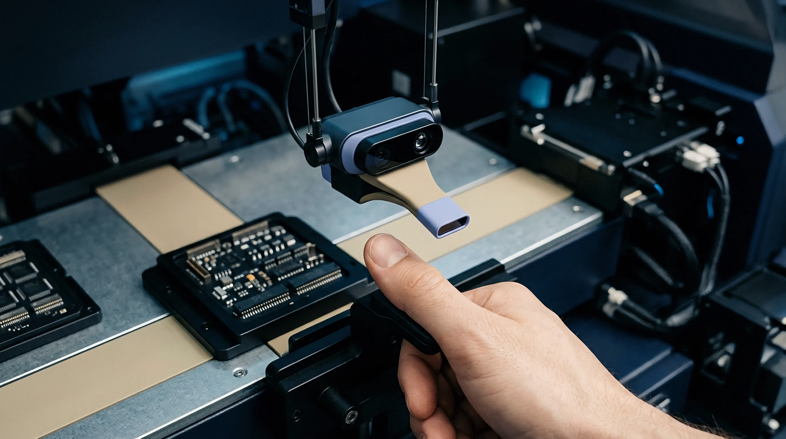
Variant
Selecting between bare LGA packages, gel-filled DFN forms, and pre-integrated PCB modules establishes both mechanical board area and long-term driver maintenance costs. One silicon die design reaches the market in five forms at five distinct price points.
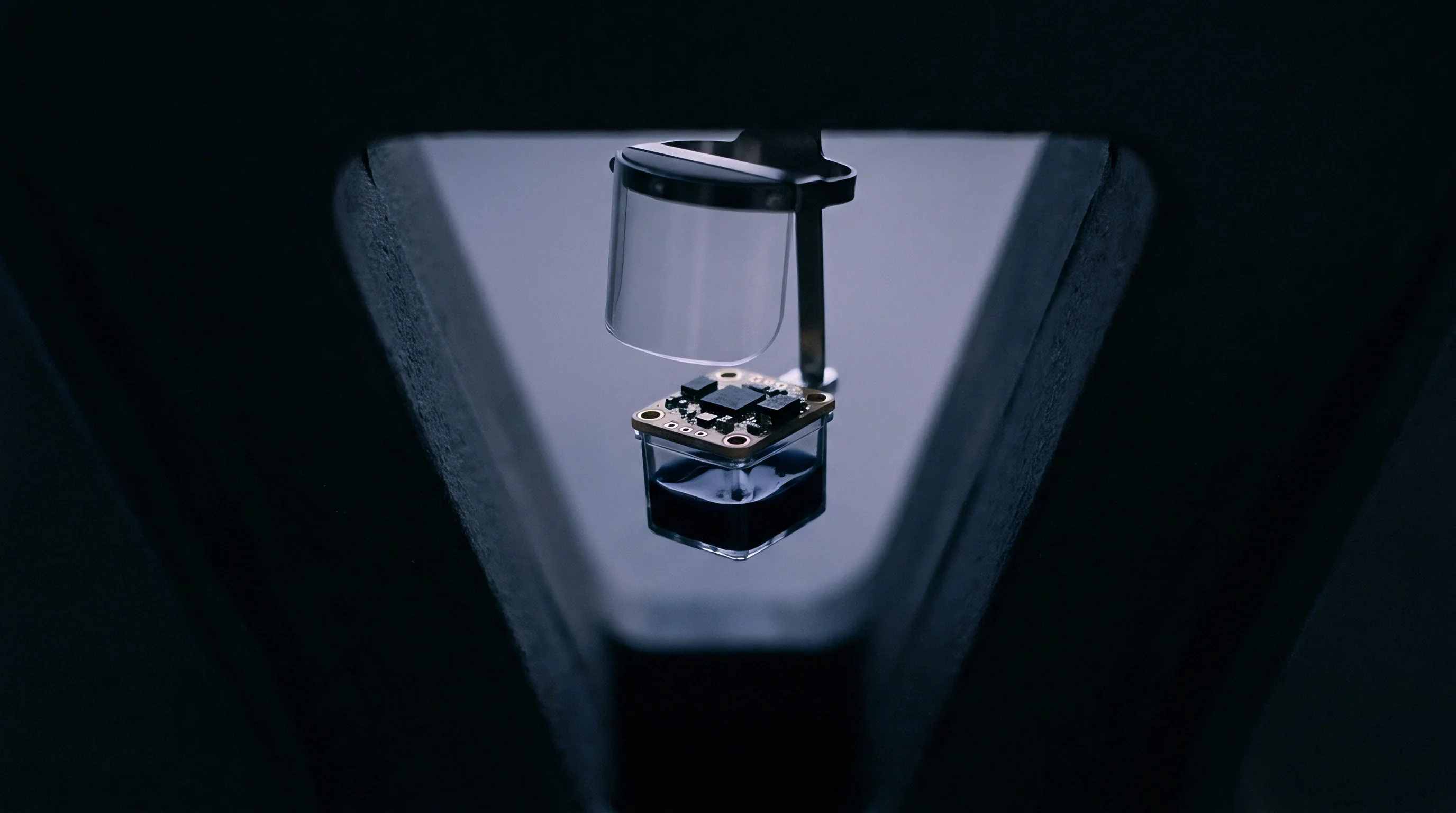
Package Form Factor Impact on Delivered Unit Pricing
One single sensor silicon design reaches the market across multiple packaging topologies with vastly different price structures. A bare LGA-8 sensor package costs $0.85 per unit at 50,000-piece volumes. The same internal silicon die packaged in a gel-filled DFN-6 enclosure for media compatibility costs $1.45 at equivalent volumes.
Gel fill cushions delicate sensor membranes. Mounting that same DFN sensor onto a small PCB module containing an onboard 32-bit microcontroller bridge elevates the unit price to $3.80 at 10,000-piece volumes. The integrated module handles all sensor conversion timing and presents a simple, fixed-rate SPI or UART interface to the main host processor, eliminating peripheral clock stretching software dependencies entirely.
Buying a cabled sensor probe eliminates board layout risk while multiplying component hardware cost by a factor of ten.

Make-or-Buy Break-Even Analysis for Clock-Stretched Sensor Modules
Engineering investment in firmware development and land-pattern qualification dictates total cost of ownership. Volume determines the optimal package selection. Module procurement eliminates firmware driver effort.
Evaluating an internal build versus external module procurement requires analyzing non-recurring engineering costs against unit volume requirements:
Option A utilizes a discrete LGA sensor package priced at $0.85. Firmware development, bring-up, and automated compliance testing demand 3 engineering weeks at $3,500 per week ($10,500). Production test fixture modification adds $15,000.
Total NRE investment equals $25,500.
Option B incorporates a pre-tested PCB sensor module priced at $3.80. Firmware integration requires 2 engineering days ($1,400), with zero test fixture NRE expenses. Total NRE investment equals $1,400.
Amortizing NRE across production runs determines the financial break-even point:
Unit Cost (Option A) = $0.85 + ($25,500 / Volume)
Unit Cost (Option B) = $3.80 + ($1,400 / Volume)
Equating both unit cost functions yields the volume break-even point:
$0.85 + ($25,500 / Volume) = $3.80 + ($1,400 / Volume)
$2.95 = $24,100 / Volume
Volume = 8,169 Units
Below 8,169 units, purchasing the pre-integrated sensor module yields lower landed costs despite higher component unit prices. Above 8,169 units, designing in the discrete LGA package and absorbing firmware driver development costs delivers progressive unit-level savings across the product lifecycle.