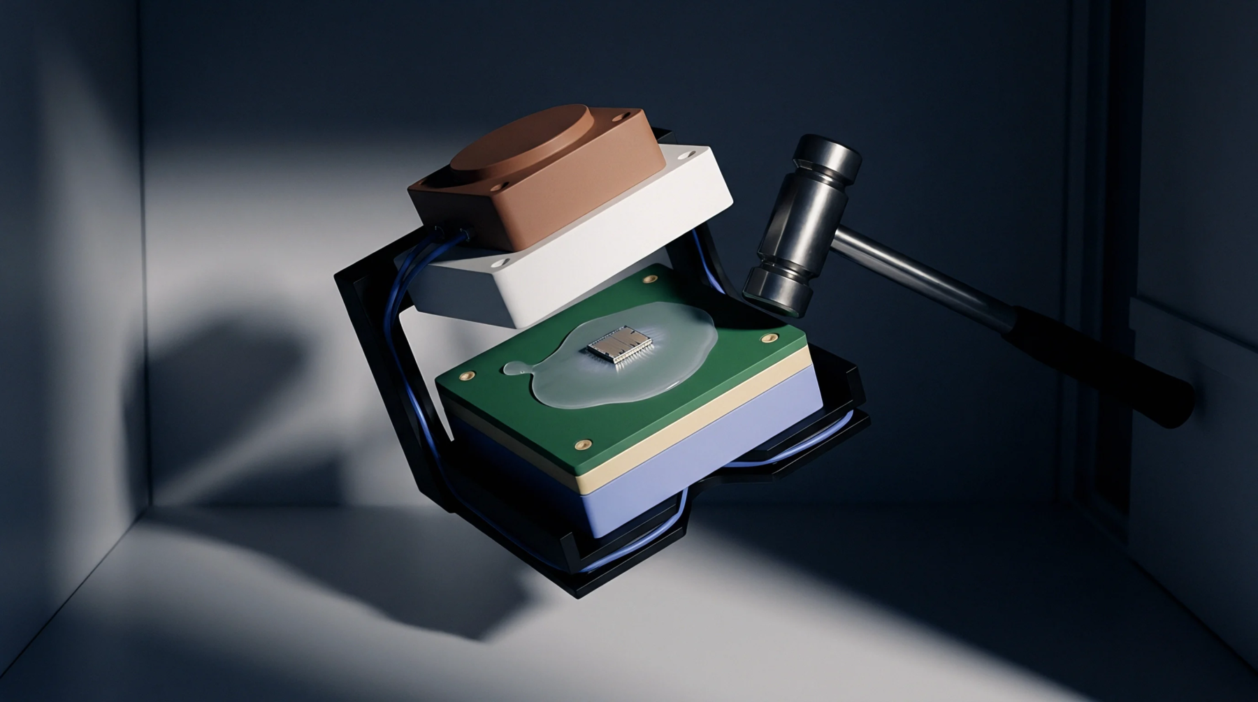
Geometric Correction
Adjusting the deposition parameters or the mechanical clamping of a semiconductor substrate counteracts the curvature induced by internal stresses. Wafer bow compensation prevents the loss of focus in lithography tools and ensures uniform contact during subsequent bonding or thinning processes. This technique manages the mismatch in thermal expansion coefficients between the silicon substrate and the various films of metal or dielectric grown upon it.
Stress Engineering
Balancing the tensile stress of one layer with the compressive stress of another allows for the maintenance of a flat profile across the entire surface. Engineers often deposit a specialized compensation layer on the backside of the wafer to provide a counteracting force. The thickness and the composition of these films are carefully tuned based on the measured deflection of the wafer after each processing step.
Metrology Feedback
Optical sensors measure the displacement of the wafer surface at multiple points to calculate the radius of curvature. This data is fed into the control system of the deposition tools to adjust the plasma power or the gas flow in real time. Accurate wafer bow compensation is required for the production of advanced three dimensional integrated circuits where multiple layers must be aligned with sub-micron precision.
Process Limit
Excessive stress can lead to the cracking of the substrate or the delamination of the active layers if the limits of the material are exceeded. The compensation strategy must therefore balance the flatness requirements against the mechanical integrity of the whole stack. Stack height affects this balance.