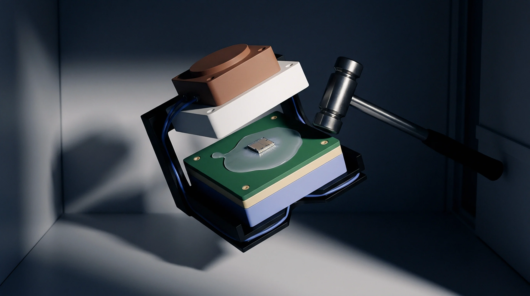
Vertical Interconnect
Vertical electrical interconnects pass completely through a silicon wafer to enable direct three-dimensional package integration. Microscopic conductive channels connect active circuitry across stacked semiconductor dies without lengthy edge wire bonds. Utilizing through-silicon vias reduces signal path lengths and minimizes parasitic capacitance between integrated circuit layers.
High-density vertical routing enables compact sensor integration in multi-die stacks.
Conductive Plating
Etched high-aspect-ratio holes through silicon substrates require uniform barrier and seed layer deposition before copper electroplating fills the cavity. Void formation during conductive metal filling increases electrical resistance and causes localized heating under high current densities. Differential thermal expansion between copper plugs and surrounding silicon generates localized mechanical stress inside the die.
Insulating dielectric liners prevent electrical leakage between conductive channels and the bulk silicon substrate. Precision etching routines maintain steep sidewall profiles to ensure uniform metallization across deep vertical channels. Four-point resistance probing verifies electrical continuity and contact resistance across thousands of vertical paths on a single wafer.
Thermal Stress
Thermal expansion mismatches between copper plugs and silicon substrates create internal stress concentrations near the via boundaries. Stress propagation alters nearby transistor mobility and shifts sensitive analogue circuit offsets. Proper thermo-mechanical design limits through-silicon vias placement distance from sensitive sensing nodes.
Continuity Verification
Electrical probe testing confirms low-resistance vertical continuity across all filled substrate channels. Acceptance criteria set maximum allowable resistance limits per vertical connection.