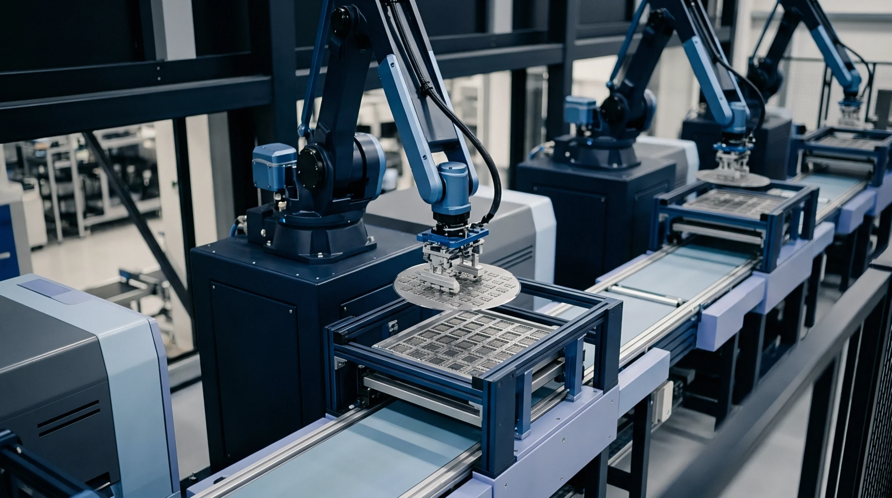
Wafers Platform
Wide bandgap semiconductor wafers used as a base for high power and high temperature electronic devices offer superior thermal conductivity compared to standard silicon. A silicon carbide substrate allows for the creation of transistors that operate at higher voltages and switch at faster speeds. These characteristics make the material ideal for electric vehicle inverters and renewable energy systems.
The crystal structure exists in several polytypes with four h and six h being the most common for electronics.
Heat Dissipation
The ability to move energy away from the active junction is nearly three times better than that of traditional materials. Devices built on silicon carbide substrate run cooler which reduces the size and weight of the necessary cooling systems. This efficiency is a primary driver for the adoption of the technology in aerospace applications.
Lower operating temperatures also extend the life of the surrounding package materials.
Mechanical Processing
Cutting and polishing the material is difficult because of its extreme hardness and brittle nature. Producing a silicon carbide substrate requires diamond tipped tools and specialized grinding slurries to achieve the necessary surface flatness. Any subsurface damage left by the machining process can lead to defects in the epitaxial layers grown on top.
The cost of production remains high due to the energy required to grow the crystals.
Quality Control
Microscopic defects known as micropipes can cause catastrophic failure in the finished power chips. Every silicon carbide substrate is inspected for crystal dislocations and impurities before it enters the fabrication line. High quality wafers are essential for achieving the high yield required for commercial success.
Standardization organizations define the allowable density of these defects for different grades of material.