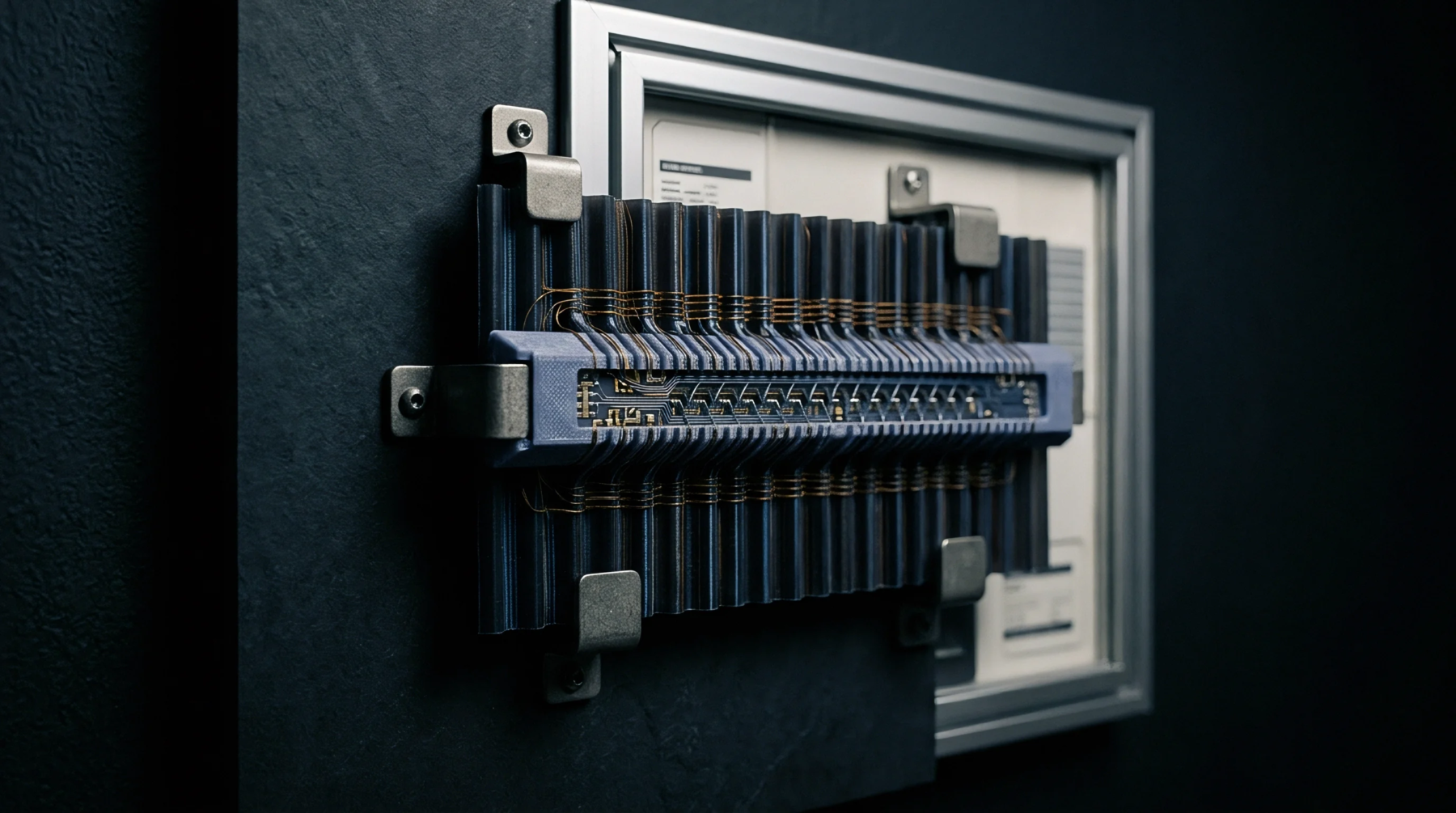
Layered Architecture
Arrangement of conductive paths and insulating materials forms the physical foundation for electronic signal distribution. A printed circuit board stackup defines the sequence and spacing of copper planes and dielectric substrates within a rigid or flexible assembly. Engineering specifications dictate these vertical profiles to manage signal integrity, power distribution, and mechanical stability.
Manufacturers verify these alignments against impedance requirements to ensure electrical performance matches design intent across high frequency applications.
Material Qualification
Dielectric constants determine the speed of wave propagation between internal layers. Variations in resin content or fiberglass weave alter the effective permittivity throughout the board. Consistent thermal expansion coefficients prevent structural delamination during repeated soldering cycles.
Engineers monitor these variables to maintain the dielectric spacing required for controlled impedance geometries.
Manufacturing Calibration
Precision etching of trace widths occurs before lamination to account for lateral copper loss. Laminating presses apply heat and pressure to bond prepreg sheets to etched cores while maintaining thickness tolerances. Laser drilling creates vertical interconnect access holes that connect specific signal planes.
Automated optical inspection verifies feature registration to detect alignment shifts that occur during the bonding process.
Performance Verification
Time domain reflectometry measures the characteristic impedance of transmission lines to validate the fidelity of the internal routing. Discontinuities in ground plane references or unexpected changes in layer separation manifest as reflection signatures during testing. Proper stackup geometry minimizes crosstalk and electromagnetic radiation by optimizing the return path for high speed digital signals.