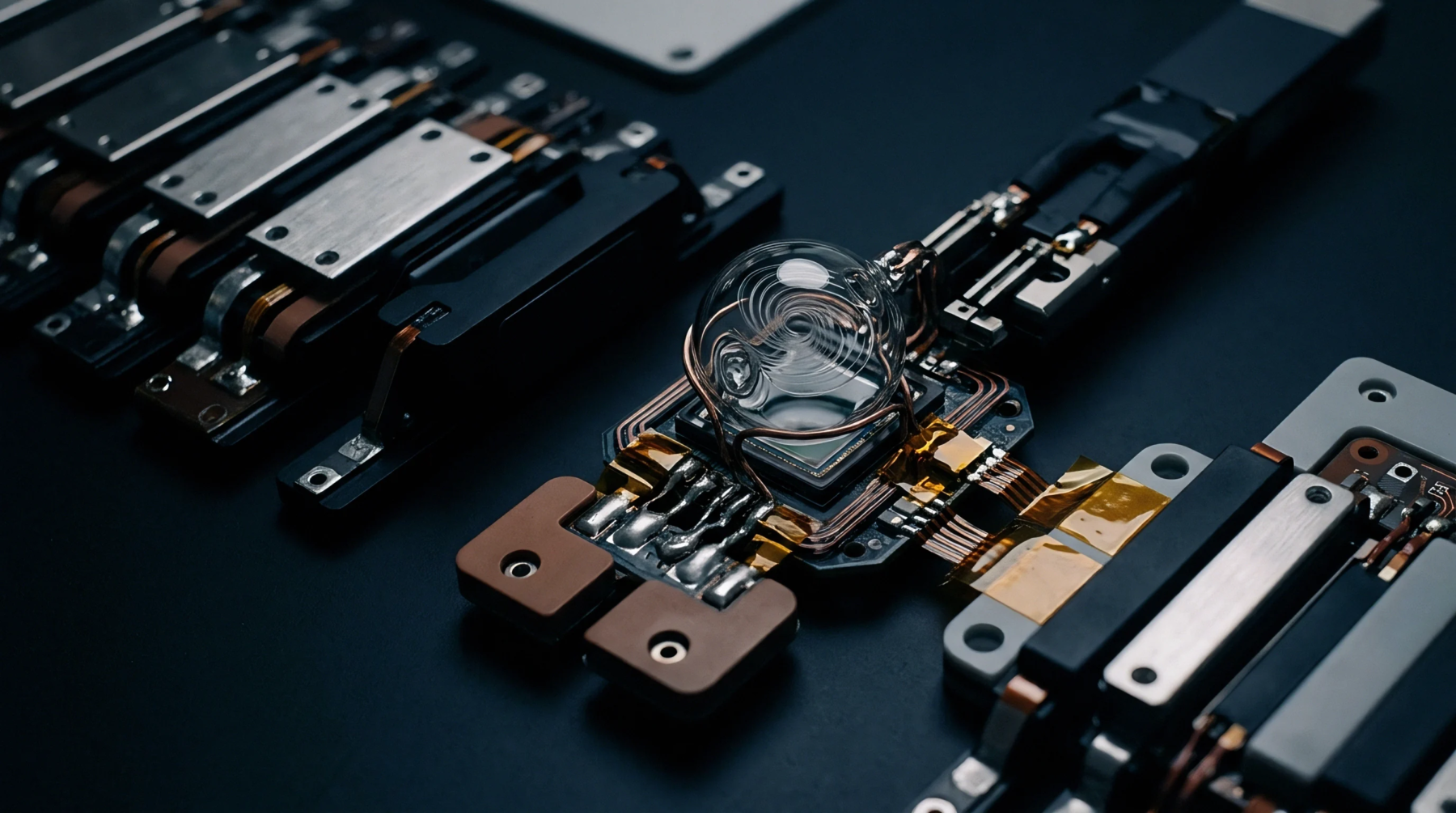
Substrate Etching
Monocrystalline material shaped through anisotropic chemical processes forms the foundation for high precision microelectromechanical transducers. Chemical reagents react along specific crystallographic planes inside micromachined silicon, yielding vertical walls and square cavities with dimensional repeatability governed by temperature and bath composition. Hydroxide solutions dissolve the crystalline lattice at rates dictated by atomic orientation, exposing the slower etching planes to create defined mechanical structures.
Calibration Drift
Residual stress gradients induced by thin film deposition degrade the long term stability of fabricated structures. Thermal expansion mismatches between the base material and metallic interconnects generate mechanical hysteresis during environmental cycling. Metrological verification requires baseline acquisition under reference conditions to quantify offset errors before deployment in operational fields.
Interference Susceptibility
Acoustic excitation couples directly into suspended mechanical elements through package housing resonances. Pressure differentials across the primary sensing boundary create offset voltages that obscure small signal measurements. Environmental isolation chambers suppress ambient vibration modes that otherwise compromise sensor accuracy during high bandwidth data acquisition.
Tolerance Verification
Metrology laboratories validate manufacturing consistency through optical interferometry and capacitive probe arrays. Primary standards laboratories establish calibration hierarchies that trace physical dimensions back to international length definitions. Subsequent manufacturing lots undergo sample testing against predefined acceptance criteria to confirm compliance with stated measurement uncertainties.